
Overview
Compatibility is a property of a named processed stack, not of a paste family or substrate label in isolation. A conductor that performs on one alumina grade can behave differently on another surface, and a resistor, dielectric, overglaze, solderable pad, or wire-bond finish introduces additional interfaces and thermal histories. Printing changes wet geometry; drying removes organics; firing or curing develops the functional film; later refires, termination, trim, protection, soldering, bonding, cleaning, coating, and assembly can change resistance, adhesion, stress, porosity, solderability, bondability, isolation, or appearance. The substrate contributes surface texture, chemistry, porosity, flatness, thermal expansion, conductivity, strength, and dimensional response. This guide turns the broad word compatibility into a verification matrix covering material identity, layer sequence, process atmosphere and profile, interactions, use conditions, measurement methods, and change control. It keeps fired ceramic thick film distinct from polymer carbon and other low-temperature printed systems, and it does not infer that a visible circuit uses a particular paste or passed a qualification test. No material option, processing range, or performance value becomes a ThickFilmPCB capability without controlled company evidence and review.
Failure controls
These are review prompts, not evidence that every risk applies or that every test is available.
- A
Combining materials because each data sheet mentions alumina while their exact grade, companion system, profile, geometry, and test methods differ
- B
Validating a conductor, resistor, dielectric, or overglaze alone and overlooking interaction after sequential firing or cure
- C
Using a supplier firing-process temperature as a finished-product operating-temperature promise
- D
Measuring initial resistance or appearance while adhesion, isolation, solder or bond interfaces, environmental drift, and failure planes remain unknown
- E
Allowing substrate finish, cleaning, furnace atmosphere, refire count, layer order, thinner, or assembly heat to change outside qualification
- F
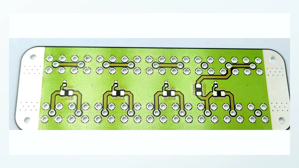
Treating a visually similar photographed circuit as proof of hidden layers, material chemistry, compatibility, electrical performance, or reliability
Engineering review matrix
Each row links a design variable to evidence that can support a drawing or release decision.
| Variable | Control question | Verification route |
|---|---|---|
| Substrate material and surface | Name grade, supplier, lot, composition evidence, thickness, flatness, texture, porosity, finish, functional face, cleaning, and storage. | Use traceable incoming records and agreed dimensional, surface, visual, and cleanliness methods. |
| Paste identity and rheology | Record material code, lot, storage, conditioning, mixing, thinner, viscosity or supplier check, screen residence, and contamination controls. | Compare receiving and process records with the current supplier documentation and printed transfer witnesses. |
| Layer order and interfaces | Define conductor, resistor, dielectric, protection, pad finish, overlaps, coverage, keep-outs, sequence, and intended chemical or mechanical interaction. | Inspect cross-sections or other agreed evidence and correlate each interface with electrical and mechanical tests. |
| Drying and firing or cure | Specify equipment, atmosphere, ventilation, part loading, time-temperature profile, peak, time at peak, cooling, repeat cycles, and permitted deviations. | Retain traceable profiles and witness results for production-intent loads; a furnace setpoint alone is insufficient. |
| Printed and final geometry | Control artwork, screen, emulsion, wet and dry dimensions, fired thickness, shrinkage or spread, edges, corners, overlaps, registration, and local defects. | Measure representative features at each critical state and correlate them to electrical and interface response. |
| Thermal and mechanical mismatch | Review CTE, modulus, thickness, substrate strength, temperature excursion, gradients, cooling, refires, joints, clamps, vibration, and shock. | Inspect and test production-intent samples before and after representative thermal and mechanical sequences. |
| Electrical and interface function | Define resistance, sheet resistance convention, TCR, current, voltage, power, isolation, leakage, solderability, bondability, contact, and noise where relevant. | Use drawing-linked methods at stated temperature, loading, geometry, and conditioning, with interface contributions separated. |
| Environment and change control | Specify humidity, condensation, fluids, contaminants, corrosion, cleaning, abrasion, storage, life sequence, material revisions, and substitution rules. | Condition the complete stack, compare baselines and failure modes, and reopen qualification when a controlled input changes. |
Controlled model
Stack compatibility and interaction model
Screen candidate stacks using thermal mismatch, target film geometry, electrical function, and layer interaction, then qualify them with production-intent coupons. Equations isolate review variables but do not calculate adhesion, crack probability, diffusion, or life from supplier typical data.
Δε_th ≈ (α_f − α_s) ΔTFirst-order free thermal-strain mismatch between a functional film and substrate over a temperature change.
- Units
- Strain dimensionless; α in 1/K or ppm/K; ΔT in K
- Use boundary
- A screening relation only. Real stress depends on elastic and viscoelastic properties, thickness, firing evolution, geometry, creep, cracking, interfaces, cooling rate, and repeated thermal history.
R ≈ R□ × L/W + R_interfacesSeparates the ideal sheet-resistance contribution from conductor overlaps, contacts, leads, and other interface effects.
- Units
- R and R_interfaces in Ω; R□ in Ω/□; L and W in the same unit
- Use boundary
- Use only for a defined fired or cured thickness and approximately uniform feature. Corners, end effects, trim, porosity, diffusion, and nonuniform processing require coupon correlation.
θ_layer = t/(kA); ΔT_layer ≈ Q θ_layerFirst-pass through-thickness thermal resistance and temperature drop of one uniform layer.
- Units
- θ in K/W; t in m; k in W/(m·K); A in m²; Q in W
- Use boundary
- Assumes one-dimensional steady conduction. Thin printed layers, contact resistance, lateral spreading, convection, radiation, and temperature-dependent properties may dominate.
S_after/S₀ = measured response after process or exposure divided by its controlled baselineA general normalized retention metric for resistance, adhesion load, isolation, or another explicitly defined response.
- Units
- Dimensionless
- Use boundary
- Never combine different measurands or methods. State conditioning, recovery, uncertainty, censoring, and failure mode before interpreting retention.
Decision comparison
| Decision | Route A | Route B | Verification |
|---|---|---|---|
| Individual material data versus complete-stack evidence | A supplier data sheet defines a named material under specific substrate, printing, profile, geometry, and laboratory test conditions. | A production stack adds other pastes, interfaces, refires, trim, protection, joining, cleaning, loads, and environmental exposure that may alter those results. | Use supplier documents for screening, then qualify the full production-intent sequence with traceable coupons and actual inspection methods. |
| Sequential versus co-fired interaction | Sequential firing can expose earlier layers to multiple thermal cycles and introduces order-dependent wetting, diffusion, stress, and surface condition. | A co-fired combination reduces some reheats but requires simultaneous compatibility of burn-out, sintering, shrinkage, atmosphere, interfaces, and final properties. | Record the exact layer order and profile for each candidate; compare properties after every relevant refire rather than after the first isolated print. |
| Ceramic firing versus polymer cure | Fired ceramic systems use inorganic pastes and a controlled furnace profile on compatible ceramic or specially insulated substrates. | Polymer systems use formulation-specific drying or cure compatible with organic or other lower-temperature substrates. | Keep bills of material, travelers, equipment, terminology, evidence, and qualification plans separate; never use an 850°C ceramic firing reference as an organic-product operating or cure claim. |
- A peak firing temperature shown in a supplier TDS describes that named material's process condition; it is not a maximum operating temperature for the finished circuit.
- Compatibility after one print is incomplete when the released route includes refires, laser trim, overglaze, soldering, wire bonding, cleaning, coating, clamping, or environmental exposure.
Complete-stack compatibility workflow
The order makes assumptions and ownership visible before a result is promoted to a requirement.
- 01
Define functions and boundaries
Map every electrical, thermal, mechanical, chemical, joining, protection, and inspection function to a layer or interface. Record reference conditions, assembly, environment, abnormal states, and failure consequences before shortlisting materials.
- 02
Lock substrate identity
Specify supplier grade, composition where legitimately documented, forming route, thickness, flatness, surface finish, functional faces, holes, edges, cleaning, storage, moisture, and incoming verification. Do not treat all alumina or AlN as interchangeable.
- 03
Construct the named material stack
List exact conductor, resistor, dielectric, overglaze, overcoat, metallization, solder, wire, adhesive, coating, thinner, and companion material codes. Review current technical and safety data and document allowed substitutions as separate qualification branches.
- 04
Sequence every process exposure
Record mixing, screen, wet dwell, leveling, drying, burn-out, atmosphere, peak, time, cooling, refires, trim, cleaning, plating if any, soldering, bonding, coating cure, rework, and storage. Identify which earlier interfaces see each later exposure.
- 05
Build diagnostic coupon coverage
Include geometry ladders, overlaps, adhesion and isolation structures, resistor and conductor witnesses, corners, vias or crossovers only when relevant, assembly pads, edge distances, and control blanks. Coupons must reflect production dimensions and support failure separation.
- 06
Measure process and functional response
Verify print and fired geometry, thickness, registration, visual condition, resistance, isolation, adhesion, solder or bond behavior, thermal response, and other drawing-linked functions with calibrated methods and declared uncertainty.
- 07
Validate and freeze the stack
Apply assembly and environmental conditions, classify failures, compare lots and tolerance cases, assign reviewers, and link the accepted stack and traveler to a drawing revision. Trigger requalification for any material, substrate, profile, layer order, or use-boundary change.
Reference boundary
Public method sources
These sources support the engineering method and terminology used in this technical guide. They do not establish a ThickFilmPCB material list, capability limit, customer result, certification, or finished-product specification.
- 01DuPont 5771 Gold Conductor technical data sheet
Supports the explicit dependency of one conductor's published behavior on a named alumina test substrate, screen, thickness, drying, firing, refires, compatible dielectric, and bond method; its data cannot qualify another stack.
- 02Heraeus C2240 Silver/Palladium Conductor technical data sheet
Supports considering paste state, printing, drying, peak firing process, fired thickness, adhesion, leach resistance, and intended application as one named test system; values remain supplier-specific.
- 03KYOCERA — Ceramic material properties
Supports that ceramic grades differ in electrical, thermal, mechanical, and processing-relevant properties; listed typical material data do not establish compatibility with any paste or ThickFilmPCB construction.
Inputs for a practical review
Unknown values may be labelled unknown. The review should convert uncertainty into an explicit decision or validation task.
Send Drawings- 01
Complete drawing and layer map with substrate grade, functional faces, conductor, resistor, dielectric, protection, terminal, joining, and interface requirements
- 02
Candidate or mandated supplier material codes, allowed substitutions, current technical data, composition or compliance documents, and storage controls
- 03
Print, dry, firing or cure, atmosphere, layer order, refires, trim, cleaning, plating, soldering, bonding, coating, rework, and assembly exposures
- 04
Geometry, registration, thickness, resistance, TCR, voltage, current, power, isolation, leakage, adhesion, solderability, bondability, and inspection criteria
- 05
Mechanical stack, contact pressure, flatness, clamps, joints, thermal mismatch, vibration, shock, edge load, and handling conditions
- 06
Operating and storage temperature profiles, humidity, condensation, fluids, contaminants, corrosion, abrasion, cleaning, and abnormal conditions
- 07
Coupon designs, prototype lots, sampling, measurement uncertainty, test sequence, acceptance rule, report format, reviewers, and change triggers