
On this page
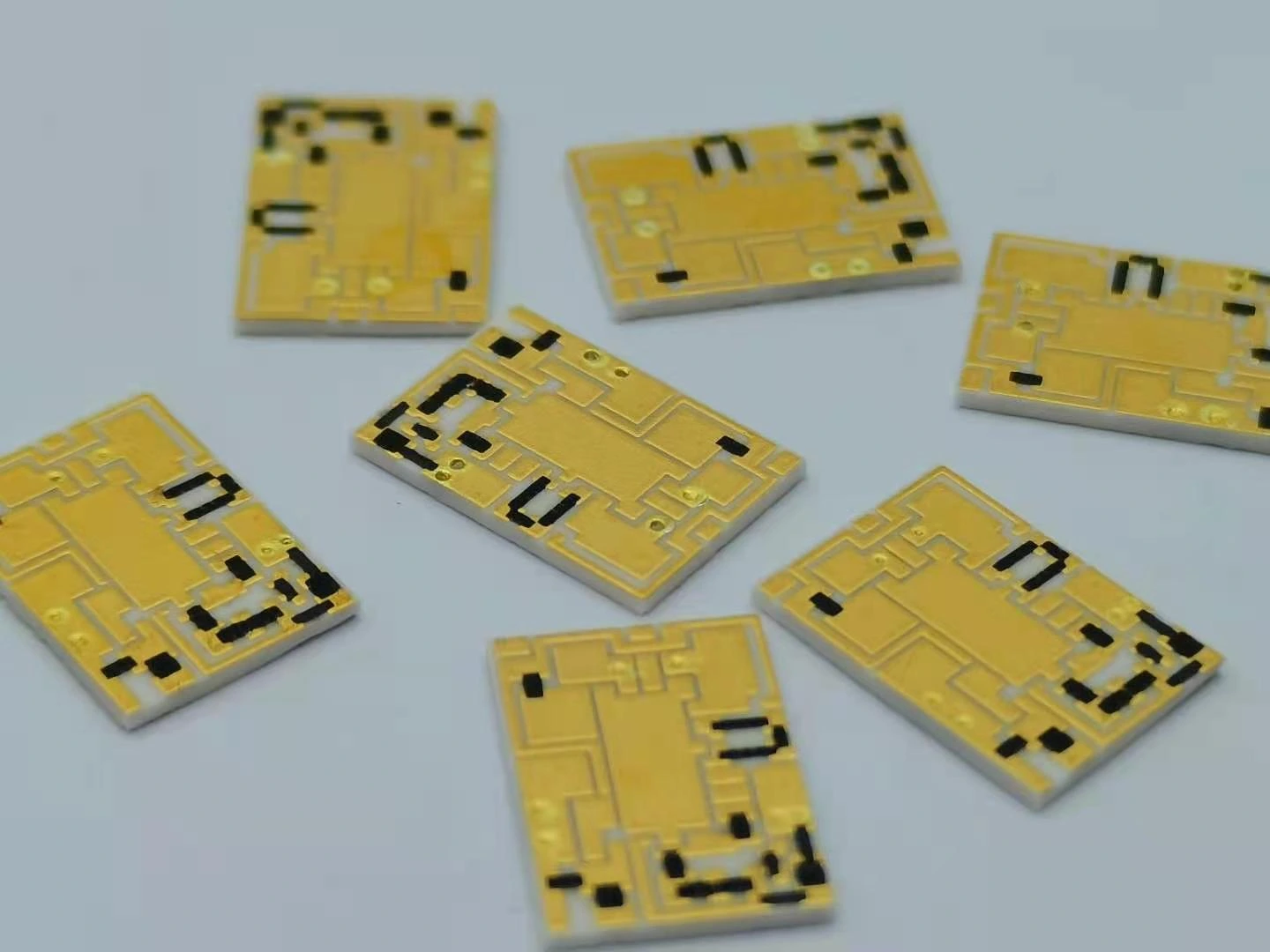
A signal attenuator needs more than the correct voltage ratio on a high-impedance meter. Its source and receiver terminations are part of the circuit. For a ceramic printed resistor pi pad, specify both port impedance and insertion loss, then calculate where the lost signal power is dissipated before choosing the physical resistor arrangement.
System boundary
A passive unbalanced symmetric pi pad between equal resistive source and load impedances. Its ideal lumped model does not establish an RF bandwidth, high-voltage rating or company attenuator product capability.
Integration interfaces
| Interface | Required input | Thick film role | Validation owner |
|---|---|---|---|
| Source to input port | Thevenin source voltage, source resistance and measurement plane. | The input shunt and series resistor establish the source loading. | Signal interface designer. |
| Output port to receiver | Receiver termination and probe loading. | The output shunt operates in parallel with the connected load. | Receiving-system owner. |
| Dissipation to ceramic layout | Continuous and transient input conditions and heat removal. | Each printed element has a different local electrical and thermal demand. | Network and thermal reviewers. |
Integration risks
| Risk | Control or verification | Validation owner |
|---|---|---|
| The attenuator is accepted with an unintended high-impedance receiver. | Verify the declared termination at both port boundaries. | Test engineer. |
| Total lost power is divided equally among unequal resistor loads. | Calculate voltage and power for each physical element. | Circuit designer. |
| DC resistor agreement is described as verified RF performance. | Measure the assembled frequency response and port match where required. | RF or analog validation owner. |
System integration decisions
- Declare the source and load impedances used to define attenuation.
- Calculate the terminated three-resistor network, not an unloaded divider.
- Allocate individual resistor dissipation and verify frequency behavior in the assembled fixture.
Define the source, load and attenuation reference
Let both the source resistance and receiver load be a positive real resistance Z. The pi pad has a series resistor Rs between its two signal ports and equal shunt resistors Rp from each port to the common return. Source resistance is outside the pad. The receiving load is connected in parallel with the output shunt, not substituted for it.
Define K greater than one as the ratio of receiver voltage without the pad to receiver voltage with the correctly terminated pad, for the same source. Attenuation in decibels is 20 log10(K). Under equal matched terminations this is also the input-port voltage divided by output-port voltage. Keep these measurement planes explicit; comparing generator open-circuit voltage directly with receiver voltage adds the source-divider effect.
Solve the matched pi network
For the stated symmetric resistive case, choose Rs = Z(K squared minus one)/(2K), and Rp = Z(K plus one)/(K minus one). These are three physical resistors: one series element and two equal shunt elements. The input resistance with the intended load attached is Rp in parallel with the series combination of Rs and the parallel pair Rp and Z.
Substituting the calculated values makes that input resistance equal to Z. By symmetry, the output resistance also equals Z when the input is terminated in the source resistance. This is why the network can preserve the nominal port match while reducing signal level. A generic voltage divider does not automatically satisfy both termination conditions, even when it produces the same measured ratio in one fixture.
Rs = Z(K^2 - 1)/(2K); Rp = Z(K + 1)/(K - 1); attenuation = 20 log10(K)
- Z: equal real source and load resistance in ohms.
- K: dimensionless terminated voltage attenuation ratio, greater than one.
- Rs: single series resistance in ohms; Rp: each shunt resistance in ohms.
Symmetric unbalanced pi pad, ideal resistors, common low-impedance return, equal real terminations and negligible parasitic effects over the evaluated band.
Verify a complete terminated example
Assume Z equals 50 ohms and choose K equal to two, corresponding to approximately 6.0206 dB. The calculated series resistor is 37.5 ohms and each shunt is 150 ohms. At the output, 150 ohms in parallel with the 50-ohm load gives 37.5 ohms. Adding the series resistor makes 75 ohms, which in parallel with the input 150-ohm shunt gives the required 50-ohm input resistance.
With an assumed source open-circuit voltage of two volts RMS and its 50-ohm series resistance, the pad input is one volt RMS. The output is 0.5 volts RMS. Without the pad, the same source would deliver one volt RMS to the 50-ohm load. The resulting ratio is exactly two in this ideal calculation. None of these values establishes an acceptable printed-resistor power or frequency rating.
Assign the lost power to its actual elements
For that example, the pad receives 20 milliwatts at its input and delivers five milliwatts to the load. It therefore dissipates 15 milliwatts internally. The input shunt dissipates one volt squared divided by 150 ohms, or approximately 6.667 milliwatts. The output shunt dissipates 0.5 volts squared divided by 150 ohms, or approximately 1.667 milliwatts.
The series element carries the current feeding the parallel output pair. Its 0.5-volt drop across 37.5 ohms produces approximately 6.667 milliwatts. The three losses sum to 15 milliwatts, but they are not equal. Assign each result to the actual printed element and thermal surroundings. Scaling the source voltage by a factor of two multiplies these ideal powers by four, while maintaining the same attenuation ratio.
| Element | Voltage across element | Calculated dissipation |
|---|---|---|
| Input shunt, 150 ohms | 1 V RMS | 6.667 mW |
| Series element, 37.5 ohms | 0.5 V RMS | 6.667 mW |
| Output shunt, 150 ohms | 0.5 V RMS | 1.667 mW |
| External load, 50 ohms | 0.5 V RMS | 5 mW, outside the pad |
Explain the apparently wrong reading with an open output
Now remove the 50-ohm load while leaving the same two-volt source and source resistance connected. The input resistance becomes 150 ohms in parallel with 37.5 plus 150 ohms, or approximately 83.333 ohms. The input voltage rises to 1.25 volts and the output becomes one volt. A high-impedance instrument therefore reads twice the previously loaded output without any resistor changing.
This is a termination change, not proof that the pad was printed incorrectly. If an instrument's input mode can switch between a termination and high impedance, record that mode with the result. Added adapters or external terminators also change the circuit. Restore the intended receiver before adjusting resistance to fix what is actually a fixture error.
Evaluate loss and impedance as separate acceptance quantities
Perturb the actual three resistance values in the terminated circuit and calculate both input impedance and receiver voltage. A coordinated change can preserve one quantity better than another. Measuring attenuation alone cannot establish a port match, and checking the three resistances independently does not automatically express the functional worst case when their errors are correlated.
Keep the actual return connection in the model. Resistance or inductance in a shared ground path can couple the two shunts and alter their effective behavior. For a ceramic network, identify which pads are input, output and common return, and which mounting or connector structures carry that return. The physical terminal mapping belongs to acceptance because an electrically similar loose resistor arrangement may not reproduce the installed interface.
Verify the assembled band instead of extrapolating from DC
The ideal resistor equations contain no frequency limit, but the real substrate, traces, pads and connections do. Parasitic capacitance and inductance change attenuation and port impedance as frequency increases. A material designation or a vendor's rating for a different packaged attenuator cannot establish the usable band of a custom thick-film network.
Use a suitable calibrated measurement arrangement at defined reference planes for the application band. Include the intended launches, return path and receiver condition, or explicitly remove fixture effects through a justified method. Preserve amplitude, phase or reflection measurements as required by the interface specification. Keep low-frequency resistance verification as a complementary check rather than presenting it as a substitute for assembled high-frequency validation.
Supply a three-part specification for the network
The drawing package should state the port impedances, attenuation and permitted input signal conditions together. Add the frequency range, termination method, return geometry and individual resistor power calculations. Distinguish continuous RMS exposure from pulses or overloads, which require their own energy and temperature review. If either end is not a real resistance Z, provide its actual impedance model instead of retaining the symmetric formula.
ChipSimple can review a drawing-defined printed resistor network with these circuit inputs. Any claimed bandwidth, power handling or assembled match requires suitable evidence for the actual construction. Repeat the terminated check after changes to connector, receiver mode, return routing or network layout so that a passing attenuation number retains the same physical meaning.
Specify the complete resistive attenuator interface
Send both terminations with the ceramic network drawing.
- Source and receiver impedance at defined reference planes.
- Target attenuation and frequency-dependent acceptance limits.
- RMS, peak and transient signal exposure.
- Input/output/return terminal geometry.
- Individual element dissipation and measurement fixture details.
The drawing-upload form loads as you reach this section.