
Overview
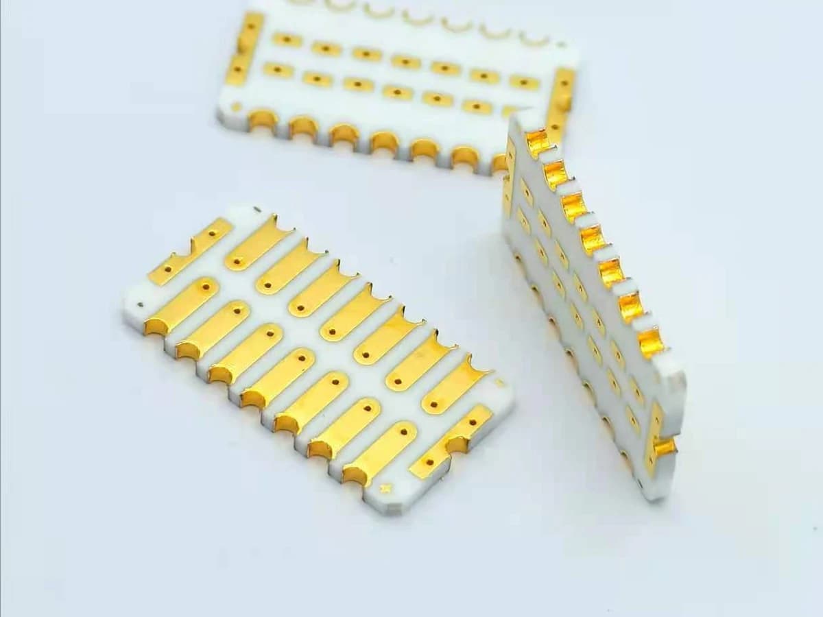
Ceramic edge clearance is the controlled distance between functional artwork and the finished edge produced by a named singulation route. this guide links saw kerf, scribe-and-break, laser cutting, or another reviewed method to datums, dimensional variation, chipping and other edge-damage zones, printed-layer setbacks, edge features, cleaning, inspection, and downstream assembly without assigning a universal clearance.
Failure controls
These are review prompts, not evidence that every risk applies or that every test is available.
- A
Artwork clearance measured from a scribe or kerf centerline while acceptance uses the finished edge
- B
Edge chipping reaching a conductor, resistor, dielectric, pad, hole, or metallized feature
- C
Edge damage remaining outside the specified visual method's sensitivity or field of view
- D
Printed films lifting, cracking, smearing, or becoming exposed during separation and cleaning
- E
Panel support, orientation, tool wear, or break direction changing the edge condition from the prototype
- F
Debris, coolant residue, or laser redeposit creating contamination or assembly interference
- G
One generic clearance being applied to features with different electrical, mechanical, and inspection risks
Finished-edge allocation method
The order makes assumptions and ownership visible before a result is promoted to a requirement.
- 01
Select the singulation route
Identify saw dicing, scribe-and-break, laser cutting, mechanical routing or milling only when validated for the specified ceramic, or another reviewed method together with panel orientation, support, entry and exit direction, sequence, and whether the functional layers are present during separation.
- 02
Set the finished-edge datum
Define whether artwork and dimensions reference the final edge, kerf centerline, scribe line, panel tooling, or another datum. Keep nominal outline, tolerance, kerf or break zone, and measurement condition distinct.
- 03
Allocate edge zones by feature
Map conductors, resistors, dielectrics, overglaze, pads, metallization, holes, slots, corner radii, and assembly contacts against process variation and the damage mode that matters to each feature.
- 04
Inspect separated samples
Use representative panels and support conditions to inspect dimensions, edge breakout, chips, cracks, burrs or redeposit, exposed films, contamination, and electrical effects with an agreed method and disposition rule.
- 05
Release artwork and acceptance together
Tie the approved singulation method, datums, feature setbacks, edge-quality criteria, cleaning, sampling, handling, packaging, and change triggers to the same drawing and revision package.
- 06
Correlate edge observations with function
Do not convert a visual chip count into an electrical-isolation, mechanical-strength, coating-integrity, or assembly conclusion without a defined correlation. Select representative worst-location indications, measure their position and extent from the finished datum, and apply only the functional checks required by the drawing risk. Retain photographs, measurement orientation, magnification, lighting, instrument method, electrical state, sample identity, and reviewer disposition. A cosmetic finding may be acceptable while a smaller indication near a loaded corner, pad, dielectric boundary, or mounting contact may require escalation.
- 07
Control variation across the panel process
Build the validation sample around panel position, substrate lot, artwork orientation, entry and exit edges, support condition, tool or beam setting, tool wear, break direction, cleaning, and handling. Compare early, middle, and later process states when the selected route can drift. The resulting evidence should show whether the proposed setback and inspection plan remain effective across the controlled process window; it must not be converted into a universal clearance for another ceramic, thickness, geometry, functional stack, panel layout, separation route, or downstream load.
Engineering review matrix
Each row links a design variable to evidence that can support a drawing or release decision.
| Variable | Control question | Verification route |
|---|---|---|
| Ceramic material and thickness | Use the specified substrate grade, thickness, surface condition, and panel form because separation response cannot be assigned from the word ceramic alone. | Confirm the received substrate record and evaluate representative processed panels. |
| Singulation method | Record tool or beam route, support, feed or break direction, sequence, coolant or dry condition, and relevant wear or maintenance controls without implying equipment ownership. | Inspect parts produced by the proposed route and retain the actual method and condition in the review record. |
| Datum and tolerance chain | Connect panel tooling, artwork registration, kerf or scribe location, break movement, finished edge, and inspection datum in one tolerance model. | Measure critical edge-to-feature distances on finished parts rather than relying only on artwork coordinates. |
| Kerf, scribe, or break zone | Define the material-removal or fracture zone, its possible asymmetry, and the area excluded from functional artwork for the selected route. | Characterize the representative finished edge and compare it with the drawing boundary. |
| Chipping and crack acceptance | Specify observable chip, breakout, corner, and crack criteria by location and function, including which indications require escalation rather than cosmetic acceptance. | Use a defined magnification, lighting, orientation, measurement rule, and disposition record. |
| Printed-layer setback | Assign separate setbacks for conductors, resistors, dielectric, overglaze, pads, and edge metallization according to exposure, stress, isolation, and assembly role. | Inspect the final edge for damaged, lifted, exposed, bridged, or contaminated functional films. |
| Edge geometry | Include corners, radii, holes, slots, notches, metallized edges, and nearby pads because they change local stress, support, and inspection access. | Evaluate the most constrained geometry in the actual panel orientation and separation sequence. |
| Post-singulation state | Define cleaning, drying, handling, storage, inspection timing, assembly contact, and packaging needed after separation. | Check visible residue, debris, film damage, dimensions, and required electrical function before release. |
Reference boundary
Public method sources
These sources support the engineering method and terminology used in this technical guide. They do not establish a ThickFilmPCB material list, capability limit, customer result, certification, or finished-product specification.
- 01KYOCERA ceramic substrate and laser-cutting design guide
Supports keeping reference edge, scribe line, substrate thickness, hole location, cutting route, and dimensional tolerances explicit in a substrate drawing; all values are KYOCERA reference data and are not transferable production limits.
- 02ASTM C1495-16(2023) — Effect of surface grinding on flexure strength of advanced ceramics
Supports the boundary that ceramic machining can introduce near-surface damage and change flexure strength, requiring material- and process-specific validation; it does not prescribe circuit edge clearance, singulation geometry, or ChipSimple capability.
Inputs for a practical review
Unknown values may be labelled unknown. The review should convert uncertainty into an explicit decision or validation task.
Send Drawings- 01
Ceramic material, thickness, panel format, finished outline, corner, hole, slot, and notch data
- 02
Proposed singulation method, panel support, orientation, sequence, and functional-layer state
- 03
Artwork registration datum and finished-part dimensional datum with tolerance ownership
- 04
Edge-to-conductor, resistor, dielectric, overglaze, pad, and metallization requirements
- 05
Electrical isolation, mechanical strength, assembly contact, and edge-exposure concerns
- 06
Chip, breakout, crack, burr, redeposit, residue, and cosmetic acceptance definitions
- 07
Inspection magnification, lighting, measurement, sampling, electrical checks, and disposition rules
- 08
Cleaning, handling, packaging, prototype panel, evidence, and change-control requirements