
Overview
Dielectric paste becomes an insulating layer only after printing and firing into a specific thickness profile over a controlled substrate and conductor geometry. Breakdown behavior depends on material, layer count, fired thickness, pores, pinholes, cracks, edges, electrode area and shape, surface paths, humidity, contamination, temperature, waveform, ramp, dwell and failure criterion. Dividing voltage by nominal thickness gives average field, not a product rating. Dielectric withstand, insulation resistance, partial discharge and long-term working-voltage design are related but distinct decisions.
Failure controls
These are review prompts, not evidence that every risk applies or that every test is available.
- A
Using voltage divided by nominal thickness as a safe field rating.
- B
Ignoring pinholes, edges, pores, cracks, particles and registration.
- C
Converting destructive breakdown into working voltage without duration/environment margin.
- D
Confusing insulation resistance, withstand and breakdown tests.
- E
Changing conductor roughness, layers, firing or protection without retest.
- F
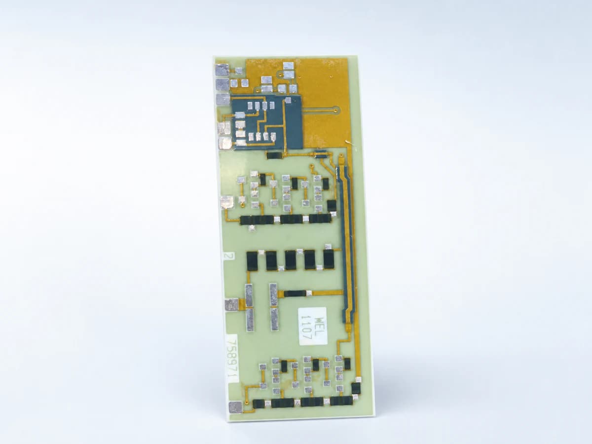
Using a photo as dielectric, voltage or qualification evidence.
Controlled model
Electric-field and defect-boundary model
Use field calculations to locate risk, then validate the complete printed stack. Average values cannot represent edges, pores, particles, cracks, electrode roughness or surface contamination.
E_avg = V/t_effAverage field across effective dielectric thickness.
- Units
- V/m
- Use boundary
- Local field may be much higher; use actual fired thickness and electrode geometry.
C ≈ ε₀ε_rA/tIdeal parallel-plate capacitance screen.
- Units
- F
- Use boundary
- Edges, pores, frequency, moisture and multilayer geometry require measurement.
Decision comparison
| Decision | Route A | Route B | Verification |
|---|---|---|---|
| One thick print versus multiple fired layers | One deposit simplifies sequence but may have thickness/profile and defect risks. | Multiple layers can offset isolated defects but add registration, interfaces, refires, stress and process time. | Section and electrically test nominal and tolerance stacks after the full sequence. |
| Coupon breakdown versus working-voltage design | A coupon test characterizes a named specimen and method to destructive failure. | Working-voltage design includes duration, transients, environment, aging, geometry, safety standard and margin. | Never convert a single breakdown statistic directly into a product working voltage. |
- Breakdown data are method- and specimen-specific; electrode area, ramp, current trip, environment and statistical treatment must accompany any value. Surface creepage around an encapsulated edge can govern even when bulk dielectric remains intact.
- Qualification should retain the distinction among a non-destructive production withstand screen, an insulation-resistance observation, a diagnostic leakage-current curve and a destructive breakdown study. Their sample plans and decision meanings are different. A high destructive value on a small clean coupon may coexist with unacceptable thin edges, registration loss or surface leakage on a large product. Conversely, a deliberately current-limited withstand test may stop without material breakdown and therefore must not be reported as dielectric strength. Product evidence should map electrode area, conductor edge shape, layer overlap, fired thickness at risk locations, defect inspection, humidity conditioning, temperature, voltage ramp, dwell, current trip, failure site and post-test condition. Statistical language also needs the actual sample population; a minimum result, average or fitted distribution cannot be exchanged casually. Any working-voltage margin must additionally include expected transients, duration, aging, contamination, accessible-metal and system safety requirements.
- When the dielectric also serves as a crossover or multilayer separator, routing and process sequence affect risk. Lower conductors can print through the surface profile, upper conductors can concentrate field at step edges, refires can change the glass and underlying layers, and vias or openings can shorten surface paths. The drawing should therefore identify every node above, below and beside the dielectric, including unused or grounded metal, and inspection should target the real overlap perimeter rather than an easy central thickness location. Assembly flux, cleaning residues, fingerprints, moisture, protective coatings, clamps and housing features can create parallel leakage routes that a bare dielectric coupon never exercises.
Dielectric-stack workflow
The order makes assumptions and ownership visible before a result is promoted to a requirement.
- 01
Define electrical boundary
List nodes, working/transient voltages, polarity, waveform, source energy/current limit, duration, ground, accessible metal, fault and application-standard ownership.
- 02
Select compatible material
Name dielectric, substrate, conductors, resistor/protection, print/fire/refire sequence, supplier revision and unresolved compatibility evidence.
- 03
Design geometry
Set layers, fired thickness, overlap, openings, edges, electrode area, corners, vias, spacing, creepage, registration and inspection datums.
- 04
Control defects
Define printing, drying, firing, cleanliness, handling and criteria for pinholes, bubbles, cracks, particles, thin edges and coverage.
- 05
Execute defined tests
Separate thickness, visual, leakage, insulation resistance, withstand, breakdown and partial-discharge intents with specimen, environment, ramp, trip and uncertainty.
- 06
Derate and control changes
Set project margin only from applicable evidence and freeze material, geometry, layers, process, environment, method and requalification triggers.
Engineering review matrix
Each row links a design variable to evidence that can support a drawing or release decision.
| Variable | Control question | Verification route |
|---|---|---|
| Voltage waveform | Define working, transient, AC/DC/pulse, frequency, polarity, dwell, source energy and fault. | Capture applied waveform and failure/current criterion. |
| Dielectric material | Name code, revision, lot, storage, substrate/conductor compatibility, firing and refires. | Retain genealogy and process records. |
| Fired thickness/layers | Set effective thickness, layer count, profile, overlap and tolerance. | Measure sections or justified thickness evidence at risk locations. |
| Defects and edges | Control pinholes, pores, cracks, particles, thin edges, registration and conductor roughness. | Inspect with defined magnification, lighting, sampling and criteria. |
| Environment | Specify temperature, humidity, condensation, contaminants, fluids, pressure and aging. | Test under relevant controlled conditions before/after exposure. |
| Surface insulation | Define creepage, clearance, protection edges, residues, ground and accessible metal. | Measure surface leakage separately from bulk behavior. |
| Test/decision method | State specimen, electrodes, area, ramp, dwell, current trip, sample size, statistics, uncertainty and margin. | Retain raw curves, locations, failures and configuration. |
Reference boundary
Public method sources
These sources support the engineering method and terminology used in this technical guide. They do not establish a ThickFilmPCB material list, capability limit, customer result, certification, or finished-product specification.
- 01ASTM D149 — Dielectric Breakdown Voltage and Strength
Supports method variables for solid dielectric breakdown; it does not create a product working-voltage rating.
- 02DuPont 7740 dielectric data sheet
Supports one named material's stated process/test context only; values are not transferable.
- 03Heraeus IP9217 dielectric data sheet
Supports named dielectric processing and typical properties only; no ChipSimple capability follows.
Inputs for a practical review
Unknown values may be labelled unknown. The review should convert uncertainty into an explicit decision or validation task.
Send Drawings- 01
Node map and working/transient voltage waveforms.
- 02
Substrate, conductor, dielectric code, layers, firing/refires and protection.
- 03
Thickness, overlap, electrode, edge, via, creepage/clearance and tolerances.
- 04
Temperature, humidity, contamination, fluids, pressure and aging.
- 05
Visual, thickness, leakage, insulation, withstand/breakdown method and criteria.
- 06
Sampling, statistics, uncertainty, margin and failure reporting.
- 07
Prototype variants, traceability, revisions, substitutions and reviewers.