
On this page
- Define the Electrical Stress Across the Dielectric
- Build Coverage with Registration Margin
- Control Pinholes and Fired Thickness
- Design Vias as Captured Interfaces
- Review Material and Firing Compatibility
- A Worked Engineering Review
- Design Review Checklist
- Questions Engineers Commonly Ask
- Related Engineering Resources
- Closing Note
Prepared by Chipsimple Engineering Team, Engineering and technical content review
Published online August 10, 2026 · Reviewed August 10, 2026
ENGINEERING ARTICLE 06 / VOLUME 1
Dielectric Crossovers and Multilayer Thick Film Circuits
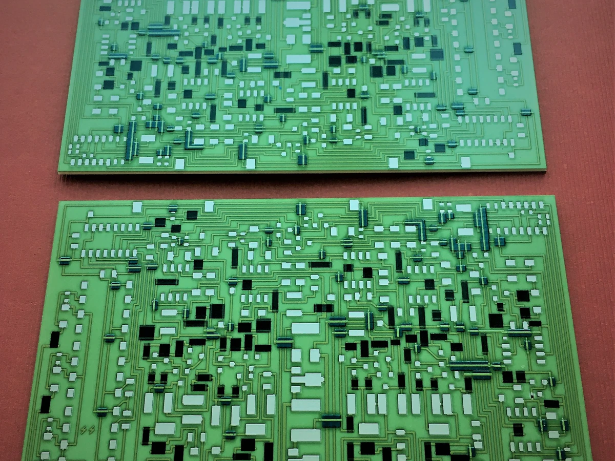
A crossover is a local multilayer structure. The lower conductor is printed and fired, dielectric is applied with enough overlap and thickness to isolate it, an opening is retained where a connection is required, and the upper conductor is printed across the insulated region. Every step changes the surface for the next. Pinholes, edge thinning, trapped contamination and poor via capture are therefore process-chain problems rather than isolated artwork defects.

Define the Electrical Stress Across the Dielectric
Geometry and material meet at this point: Dielectric thickness alone does not define isolation. Therefore, working voltage, transient waveform, conductor edge shape, overlap, defects and environment determine electric-field stress. A nominal specification that omits the interface is incomplete even if every individual value looks reasonable.
During release, state working and test voltage, polarity, transient duration and insulation-resistance requirement. Make sure the acceptance method measures the same physical feature that the design calculation assumed.
Useful confirmation includes withstand and leakage testing on structures representative of the smallest overlap and dielectric window. Keep photographs or sections tied to part, revision, lot and orientation so they remain evidence rather than decoration.
One failure signature is breakdown at a conductor edge even though average printed thickness meets the target. It often becomes clear only when results are sorted by position, process stage or exposure instead of being combined into one average.
Build Coverage with Registration Margin
Process capability follows from the mechanism: The dielectric must continue beyond the lower conductor after worst-case layer displacement. The direct implication is that insufficient overlap can expose an edge or leave a thin wedge that becomes the preferred leakage path. This makes the topic a design input, not merely a factory setting adjusted after the drawing is complete.
A practical release action is to specify minimum remaining dielectric overlap and use qualified print compensation. The requirement should survive staff changes and future lot reviews because it is recorded with the controlled construction.
Use overlay inspection before the upper conductor hides the interface to demonstrate margin. When feasible, compare the result before and after the operation most likely to disturb it.
Pay attention to intermittent high leakage concentrated on one side of the crossover. A corrective action is credible only when it changes that physical mechanism and the follow-up data confirm the change.
Control Pinholes and Fired Thickness
Multiple dielectric prints may be used to improve coverage and reduce through-defect alignment. The consequence is that one heavy print can dry or fire differently from a controlled multi-print build. In a thick film dielectric crossover review, this relationship deserves an explicit decision rather than an assumption copied from a previous drawing.
The practical control is to qualify print count, drying and firing sequence with the selected dielectric and conductor system. That instruction should be linked to the layer, material system or feature it governs so that production and inspection read it in the same way.
Verification should include coupon thickness, optical inspection and electrical testing after each critical dielectric build. If the evidence is collected only after final assembly, the team loses the ability to separate printing, firing, trimming and assembly effects.
A common warning sign is pinholes, blistering, cracks or incomplete burnout beneath the next layer. Treat that symptom as a request to examine the process chain, not simply as a reason to widen the final tolerance.
Design Vias as Captured Interfaces
A via opening needs reliable contact to both connecting conductors. The consequence is practical: small openings, misregistration and poor paste fill can create continuity with unstable resistance. This is one reason thick film dielectric crossover cannot be reduced to a single catalogue value.
During design review, provide sufficient land, controlled opening geometry and an agreed via-fill or print method. The objective is not to freeze every process setting on the customer drawing, but to define the functional boundary that the manufacturer must protect.
A useful evidence package contains four-wire via-chain resistance, cross-sections and thermal-cycle monitoring. Comparing those records with the approved construction is more informative than judging an isolated photograph or one resistance reading.
Watch for via resistance that rises after cycling while the rest of the conductor network remains stable. It often indicates that two individually acceptable variables have combined at the edge of their windows.
Review Material and Firing Compatibility
Each additional firing exposes previous layers to another thermal cycle. Consequently, re-firing can change conductor morphology, resistor value, dielectric stress and interface adhesion. The engineering value comes from understanding the direction and sensitivity of the effect, not from memorising a nominal number.
A robust drawing or process plan will use a qualified material family and plan the complete print-fire order before tooling. This makes the design intent visible and gives the supplier room to use a qualified material set without changing the function.
The result can be checked through layer coupons measured at key stages and final cross-sections from qualification builds. Where possible, keep readings before and after the next thermal or mechanical operation; the delta often reveals more than the final value.
The failure pattern to investigate is a later layer fixing one defect while degrading an earlier electrical characteristic. Before changing materials, confirm orientation, lot history, measurement method and acceptance limits.
A Worked Engineering Review
For one signal crossover, the first question is whether a simple route change can remove the multilayer feature. If not, define the lower conductor width, dielectric overlap and upper conductor width using the process registration window. Select a dielectric build that meets isolation after firing, not only when wet. Add a coupon containing the minimum overlap and, if vias are present, a daisy chain. Inspect the dielectric before covering it, then test leakage and continuity after the upper conductor fire. For a network of many crossovers, statistical coupon evidence becomes more valuable than inspecting one attractive micrograph.
Design Review Checklist
- Specify working voltage, transient and test method.
- Define minimum dielectric overlap at worst-case registration.
- Qualify print count, dried state and firing sequence.
- Use captured via lands and measurable via chains.
- Inspect critical dielectric before it becomes buried.
Questions Engineers Commonly Ask
Is one dielectric print enough?
It can be for a qualified low-stress structure, but print count is a process decision. Multiple prints may improve defect coverage; they also add thickness and thermal cycles. Qualification should use the actual construction.
Can a crossover be tested only for continuity?
No. Continuity checks the conductor path, not dielectric isolation. Include insulation resistance or withstand testing appropriate to the voltage and environment.
Why are via chains used on coupons?
A chain amplifies small resistance changes and gives a measurable indicator of via process consistency. It is especially useful before individual vias become inaccessible in the finished circuit.
Related Engineering Resources
Closing Note
Successful multilayer thick film is built through controlled interfaces. The layout, material family, print-fire sequence and evidence plan must be reviewed together before the first screen is made.