
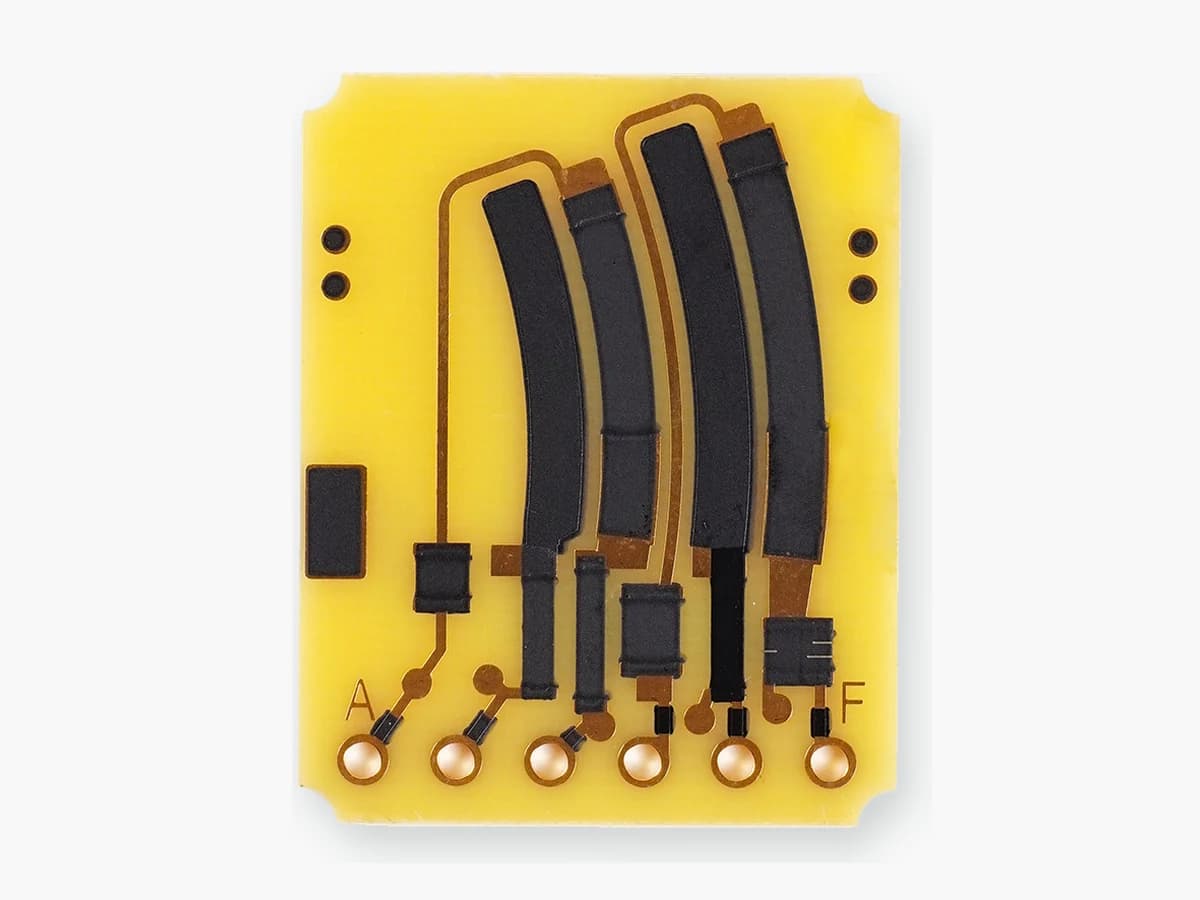
Overview
Polymer thick-film carbon ink is a family of printable functional materials, not a drop-in black coating. Selection begins with the intended function: a resistive element, low-current conductor, contact surface, jumper, potentiometer track, sensor electrode, shielding feature, or another defined task. Each task places different weight on sheet resistance, contact behavior, surface texture, adhesion, flexibility, abrasion, chemical exposure, printing window, cure, compatible silver or dielectric layers, and long-term change. The polymer route normally uses a supplier-defined drying or curing cycle compatible with an organic film or printed-board substrate; it must not be described as the high-temperature firing route used for classic ceramic thick film. Supplier data are also formulation- and test-construction-specific. A value measured on polyester at a stated thickness cannot establish resistance on FR4, polyimide, polycarbonate, an unfamiliar surface treatment, or a production geometry. This guide converts the material choice into a controlled stack, process, geometry, contact system, and validation plan. It makes no public claim that a photographed circuit uses a named ink or that ThickFilmPCB has qualified any unlisted resistance, flex, wear, chemical, temperature, or life condition.
Engineering review matrix
Each row links a design variable to evidence that can support a drawing or release decision.
| Variable | Control question | Verification route |
|---|---|---|
| Functional mode and measurand | Define fixed resistance, contact resistance, transfer function, electrode response, or conductivity and the exact nodes and conditions. | Use a fixture and method that separates body, termination, lead, probe, and moving-contact contributions where required. |
| Substrate and surface chemistry | Name the laminate or film, resin, copper finish, treatment, roughness, cleanliness, moisture state, and storage history. | Run wetting, adhesion, dimensional, visual, and electrical coupons on the production-intent surface and lot range. |
| Ink identity and condition | Record manufacturer, product code, lot, shelf state, storage, conditioning, mixing, thinner, open time, screen residence, and contamination controls. | Use supplier documentation, receiving records, viscosity or other agreed checks, and lot-linked traveler data. |
| Printed and cured geometry | Specify artwork, effective L/W, end overlap, corners, conductor registration, cured width, thickness, profile, pinholes, and local necks. | Measure coupons after cure and correlate actual geometry with resistance distribution and microscope inspection. |
| Cure and thermal history | Define oven type, air flow, time-temperature profile, support, loading, solvent removal, repeat cure, later reflow, lamination, overmolding, or adhesive cure. | Record part-level or representative profile evidence and compare mass, resistance, adhesion, and appearance after each relevant stage. |
| Electrical and thermal loading | State voltage, current, power, pulse, duty, source and load impedance, local heat path, ambient, and fault behavior. | Measure voltage and temperature distribution on production-intent geometry through nominal, tolerance, startup, and abnormal states. |
| Contact and wear system | Define wiper material and shape, force, speed, direction, travel, cycles, vibration, contamination, lubrication prohibition or allowance, and contact-current mode. | Capture dynamic output, contact resistance, noise, debris, track wear, and post-test microscopy at specified intervals. |
| Environment and protection | Specify humidity, condensation, fluids, cleaners, fuels, sulfur, salts, abrasion, UV, coating, coverlay, seal, and edge exposure. | Condition complete coupons or assemblies and compare electrical, mechanical, visual, and contact baselines with recovery time stated. |
Controlled model
Printed carbon resistance and use-condition model
Use sheet resistance to size an initial straight feature, then add termination, contact, cure, thickness, geometry, temperature, strain, wear, humidity, and aging effects. The model is a starting point for coupons; it does not replace production-intent testing.
R_body ≈ R□ × (L/W)First-order body resistance of a uniform rectangular printed carbon element expressed through its number of squares.
- Units
- R_body in Ω; sheet resistance R□ in Ω/□; L and W in the same length unit
- Use boundary
- Assumes uniform thickness, bulk behavior, straight current flow, and negligible end effects. Supplier sheet resistance applies only at its stated substrate, cure, thickness, and method.
R_total = R_body + R_end,1 + R_end,2 + R_contactSeparates the ideal printed body from conductor overlaps, probe or wiper contact, and other interface contributions.
- Units
- All terms in Ω
- Use boundary
- Terms can be nonlinear, pressure-dependent, position-dependent, and time-varying; identify the measurand and fixture before assigning values.
P = I²R = V²/R; q'' = P/A_activeRelates electrical loading to total dissipation and nominal active-area power density for screening.
- Units
- P in W; q'' in W/mm² or W/m²; V in V; I in A; R in Ω
- Use boundary
- Does not predict local temperature, current crowding, contact heating, allowable power, or life. The assembly heat path and material limits require analysis and test.
ΔR/R₀ = (R_conditioned − R₀)/R₀Normalizes resistance change after cure, flexing, wear, humidity, chemicals, assembly, or aging.
- Units
- Dimensionless, commonly %
- Use boundary
- State conditioning, elapsed time, measurement voltage, temperature, contact method, and recovery time. A reversible response and permanent change must not be combined.
Decision comparison
| Decision | Route A | Route B | Verification |
|---|---|---|---|
| Resistive body versus sliding contact | A fixed resistor prioritizes value distribution, geometry, loading, thermal path, stability, and compatible termination overlap. | A wiper track also prioritizes surface texture, contact force, wiper material, speed, travel, debris, bounce, wear path, and output noise. | Use different coupons and test methods for body resistance and dynamic contact performance; a static ohmmeter reading cannot release a potentiometer track. |
| Organic polymer route versus fired ceramic thick film | Polymer carbon systems are selected with an organic substrate, solvent interaction, drying or cure, flexibility, overprint, and assembly-temperature boundary. | Classic ceramic thick film uses inorganic material systems and supplier-defined firing profiles on compatible ceramic surfaces. | Keep material lists, process travelers, terminology, qualification coupons, and change control separate; do not transfer an 850°C firing condition to an organic carbon-ink product. |
| Lower versus higher nominal sheet resistance | A lower sheet resistance may reduce square count but can change formulation behavior, contact response, geometry sensitivity, blending strategy, and process window. | A higher sheet resistance may support compact high values but can increase voltage, noise, end-effect, thickness, and environmental sensitivity for the chosen function. | Print a geometry ladder and functional coupon using each candidate system, then compare distribution and use-condition response against the same acceptance plan. |
- Record whether resistance is normalized to dry or cured thickness and whether the supplier reports Ω/□, Ω/□/mil, or another thickness convention.
- Contact tracks require tribology and dynamic electrical evidence; a carbon formulation described as conductive or abrasion resistant does not automatically fit a wiper system.
Polymer carbon material-selection workflow
The order makes assumptions and ownership visible before a result is promoted to a requirement.
- 01
Define the printed function
State whether the carbon is a fixed resistor, sliding track, contact finish, jumper, electrode, shield, or another feature. Record the electrical circuit, acceptable change, safety consequence, measurement method, and interaction with conductors, dielectrics, coatings, adhesives, and mechanics.
- 02
Lock substrate and surface
Identify FR4, polyester, polyimide, polycarbonate, or another exact substrate construction, copper or finish state, surface treatment, cleanliness, roughness, flexibility, thickness, dimensional change, and maximum process exposure. Similar polymer names do not guarantee solvent or cure compatibility.
- 03
Review the named material system
Use current supplier data and safety documents to compare intended application, sheet resistance convention, rheology, solids, thinner, screen, wet hold, drying or cure, thickness, adhesion, abrasion, companion materials, storage, and limitations. Do not create a hybrid recipe from unrelated data sheets.
- 04
Design geometry and interfaces
Calculate a starting square count, then design end overlaps, corners, necks, probe lands, wiper transitions, registration, print direction, thickness target, current path, wear path, trim or calibration, coverlay, and keep-outs around later assembly operations.
- 05
Build process-representative coupons
Print candidate geometries with production-intent screen, ink lot, mixing, printing, dwell, cure, substrate support, companion layers, overprints, assembly heat, cleaning, and storage. Record actual cured dimensions and thickness rather than assuming artwork equals the conductive body.
- 06
Validate and control change
Test electrical, contact, mechanical, environmental, and aging responses with agreed fixtures and uncertainty. Release the complete construction to one drawing and reopen review after any ink, substrate, pretreatment, screen, cure, wiper, coating, adhesive, cleaning, or assembly change.
Failure controls
These are review prompts, not evidence that every risk applies or that every test is available.
- A
Using a supplier sheet-resistance value without matching substrate, cured thickness, cure profile, print method, temperature, and measurement convention
- B
Calling an organic low-temperature cure a ceramic firing process or mixing polymer carbon and fired ceramic thick-film evidence
- C
Treating a static body-resistance coupon as proof of sliding-contact noise, wear, debris, output smoothness, or cycle life
- D
Ignoring solvent attack, dimensional change, moisture, copper finish, surface treatment, later reflow, lamination, adhesive, or overmolding
- E
Relying on nominal artwork while cured width, edge profile, thickness, overlap, pinholes, or registration control the real current path
- F
Allowing ink substitution or thinner adjustment without repeating compatibility, electrical, contact, mechanical, and environmental review
Reference boundary
Public method sources
These sources support the engineering method and terminology used in this technical guide. They do not establish a ThickFilmPCB material list, capability limit, customer result, certification, or finished-product specification.
- 01DuPont 7105 Carbon Conductive Composition
Supports the need to bind carbon-ink properties to a named polyester test construction, screen, cured thickness, cure, resistance convention, adhesion, abrasion, storage, and stated limitations; it is not evidence for FR4 or ThickFilmPCB capability.
- 02DuPont ME201 Carbon Conductor
Supports formulation-specific substrate, thermoforming, overmolding, printing, cure, thickness, adhesion, and resistivity considerations for one in-mold-electronics material only; values must not be transferred to another carbon system.
- 03IPC-7092 official table of contents
Supports that printed-electronics implementation treats PTF resistor geometry, land compensation, curing, testing, coupons, and reliability as linked design topics; detailed contractual criteria require the licensed current standard.
Inputs for a practical review
Unknown values may be labelled unknown. The review should convert uncertainty into an explicit decision or validation task.
Send Drawings- 01
Circuit and mechanical drawings identifying printed function, nodes, end-to-end value or transfer target, active area, contacts, and inspection datums
- 02
Exact substrate construction, copper or finish state, pretreatment, thickness, flexibility, forming, dimensional tolerance, and process-temperature limits
- 03
Candidate or prohibited carbon inks, companion silver or dielectric layers, coating, adhesive, coverlay, overmold, and material-compliance needs
- 04
Voltage, current, power, pulse, duty, source and load impedance, measurement current, calibration, and allowable initial and conditioned change
- 05
For contacts: wiper material, geometry, force, speed, travel, cycles, direction, vibration, contact current, noise, bounce, and debris limits
- 06
Humidity, condensation, fluids, chemicals, cleaning, abrasion, UV, storage, thermal cycling, assembly, and recovery conditions
- 07
Prototype quantities, coupon matrix, sampling, test methods, acceptance rules, traceability, report format, and change-control triggers