
Overview
Post-fired thick-film circuits, high-temperature co-fired ceramic and low-temperature co-fired ceramic are different manufacturing architectures, not interchangeable labels for a ceramic circuit. Conventional thick film adds printed conductors, resistors, dielectrics or protection to an already fired substrate through one or more print and fire steps. HTCC and LTCC build multilayer ceramic bodies from green tapes or related forming routes with internal conductors and vias that are co-fired under system-specific conditions. The correct choice depends on where routing and passive functions must reside, layer count, interconnect density, material compatibility, shrinkage control, thermal path, hermetic or package boundary, surface assembly, volume, tooling, inspection, repair, supply-chain maturity and validation. This page makes no claim that ChipSimple manufactures HTCC or LTCC.
Engineering review matrix
Each row links a design variable to evidence that can support a drawing or release decision.
| Variable | Control question | Verification route |
|---|---|---|
| Interconnect architecture | Define layer count need, internal versus surface nets, crossovers, vias, grounds, shields, cavities, feedthroughs, test points, trim access and repair access. | Review net-to-layer traceability and inspect/test representative internal and external interconnects using route-appropriate methods. |
| Named ceramic/material system | Identify fired substrate or green tape, conductor, resistor, dielectric, via fill, seal/finish, supplier revisions, firing atmosphere, compatibility and substitutions for each route. | Retain supplier-controlled documentation and material/process genealogy with representative construction and measured results. |
| Geometry and dimensional control | Set finished outline, thickness, flatness, holes, cavities, layers, line/gap, vias, pads, registration, fired dimensions or directional shrinkage compensation and tolerance stack. | Measure finished configuration and, for co-fired routes, correlate green, laminated and fired data through the supplier's controlled process. |
| Electrical and passive behavior | Allocate conductor/via resistance, current, voltage, isolation, parasitics, resistor values, tolerance, TCR, VCR, noise, stability, trim/calibration, contacts and test loading. | Test the complete loaded circuit across stated voltage, current, frequency, temperature and environmental conditions. |
| Thermal and mechanical boundary | Define sources, duty, substrate/body properties, internal paths, vias, interfaces, heat sink, package, mounting, CTE, stress, warpage, vibration, shock and thermal cycling. | Correlate analysis with mapped production-intent assembly temperatures and pre/post mechanical/thermal inspection. |
| Assembly and package interfaces | Specify die/component attach, wire bonding, solder/adhesive pads, finishes, leads, feedthroughs, seals, encapsulation, cleaning, rework, surface state and downstream heat. | Qualify exact interface stacks after the full circuit and package process sequence and relevant exposures. |
| Supply, evidence and change control | Define design-rule authority, supplier qualification, prototypes, tooling, traceability, internal-feature inspection, electrical tests, reports, capacity/lead evidence if needed, revisions and change notification. | Audit the selected supplier's configuration-linked evidence and reopen review after material, tooling, process, design-rule, site or architecture changes. |
Controlled model
Architecture-boundary comparison
Compare the routes from the same electrical, mechanical, thermal, package and supply requirements. Bulk ceramic properties and nominal line-width tables are insufficient: the process architecture determines internal access, material choices, shrinkage, surface state, resistor strategy, vias, cavities, assembly and inspection. Values must come from the named supplier/process and be verified in the selected construction.
R_path = Σ(ρ_i L_i/A_i) + ΣR_interfaceFirst-order electrical resistance budget through conductors, vias and interfaces in any selected architecture.
- Units
- Ω
- Use boundary
- Effective resistivity, fired geometry, temperature, current crowding, via construction, contacts, surfaces and process variation require route-specific data and measurement.
θ_path ≈ Σ[t_i/(k_i A_i)] + Σθ_interfaceOne-dimensional screen for thermal resistance through layers and interfaces.
- Units
- K/W
- Use boundary
- Real circuits include lateral spreading, vias, cavities, anisotropy, local sources, metallization, mounting, convection, radiation and temperature-dependent properties.
D_fired = D_green(1 − S)Simple relation between a green feature and fired dimension using fractional shrinkage.
- Units
- Length; S dimensionless
- Use boundary
- Relevant only to a defined co-fired process with controlled directional shrinkage. Actual x/y/z shrinkage, pattern interaction, lamination, material lot, loading and warpage need supplier/process evidence.
Decision comparison
| Decision | Route A | Route B | Verification |
|---|---|---|---|
| Layer formation and design commitment | Post-fired thick film starts with a fired substrate and adds surface layers, crossovers or selected vias sequentially; later prints remain accessible but every firing and interface must stay compatible. | HTCC/LTCC create internal layers, vias and possibly cavities before co-firing; they enable buried architecture but require early commitment to tape, metallization, lamination, shrinkage and internal inspection strategy. | Review actual cross-sections, material declarations, process flow, design rules and representative build evidence from the intended supplier; do not infer internal architecture from an exterior image. |
| Conductor and passive integration | Post-fired thick film can print conductors and resistors on accessible fired surfaces and use dielectric crossovers or multilayer sequences where qualified. | Co-fired routes can embed conductors and selected passive structures, but available metals, resistors, dielectrics, firing atmosphere and tolerances depend on the named HTCC or LTCC system. | Compare the real netlist, resistor/element tolerance, trim access, current, RF/parasitic, thermal and test needs with supplier-controlled material systems. |
| Thermal and package boundary | A fired substrate route exposes surfaces for printed heat paths, components, sensors and mounting, with thermal performance governed by substrate, layers and interfaces. | A co-fired body can integrate vias, cavities and package features, but its effective heat path, seals, feedthroughs, internal conductors and assembly surfaces remain construction-specific. | Model and measure the complete source-to-sink assembly at common power, mounting, ambient and fault conditions; bulk conductivity does not select the route. |
| Prototype change versus production integration | Accessible sequential layers may support quicker artwork or surface-functional iteration, while process compatibility and repeated firings still constrain changes. | Integrated multilayer tooling and co-firing can suit a stable architecture but design changes may affect tapes, screens, vias, cavities, lamination, shrinkage compensation and qualification. | Request supplier-specific non-recurring work, revision control, sample plan, inspection, yield evidence where approved, capacity and change lead implications without publishing unsupported promises. |
- High-temperature and low-temperature in HTCC and LTCC name co-firing families; those labels must not be presented as finished circuit operating-temperature ratings. Likewise, a thick-film paste firing condition, including any supported 850°C process reference, is not product service temperature.
- The most integrated route is not automatically the best. Test access, trim access, repair, component replacement, material sourcing, process maturity, inspection of buried features, model correlation, revision cost, package ownership and qualified supplier evidence can outweigh nominal layer density.
Failure controls
These are review prompts, not evidence that every risk applies or that every test is available.
- A
Using thick film, HTCC and LTCC as marketing synonyms and accidentally merging post-fired, high-temperature co-fired and low-temperature co-fired materials or capabilities.
- B
Selecting from generic line width, layer count, conductivity or temperature tables without the named supplier's compatible tape, metal, via, firing, shrinkage and inspection system.
- C
Assuming embedded layers and cavities automatically improve density, thermal performance, hermeticity, cost, yield or reliability without the full construction and package boundary.
- D
Choosing post-fired accessibility without budgeting repeated firing compatibility, crossover/via complexity, registration, surface area, trim, protection and assembly interactions.
- E
Ignoring how buried-feature inspection, destructive analysis, test access, rework, design changes, tooling, supplier maturity and qualification affect program risk.
- F
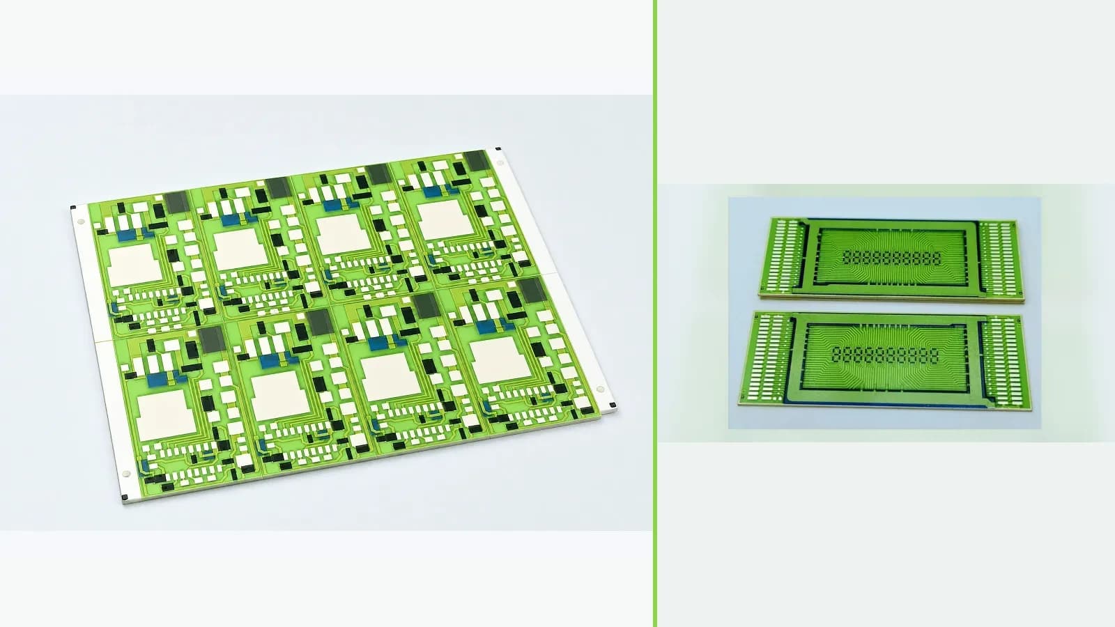
Using a photograph of post-fired thick-film samples as visual evidence of HTCC/LTCC construction or of ChipSimple co-fired manufacturing capability.
Ceramic architecture selection workflow
The order makes assumptions and ownership visible before a result is promoted to a requirement.
- 01
Freeze functional architecture
Document netlist, analog/digital/RF behavior where applicable, resistance and ratio functions, current and voltage, layer crossings, grounds and shields, thermal sources, component/die/wire interfaces, external pads, outline, cavities, package, environment, service and system verification.
- 02
Separate process families
Draw a post-fired thick-film route on a fired substrate separately from HTCC and LTCC green-body, printing, via filling, stacking, lamination and co-firing routes. Name the supplier/material system for each; do not combine favorable properties from unrelated systems.
- 03
Map materials and design rules
For each route, list ceramic or tape, conductors, resistors, dielectrics, vias, cavities, seals, surface finish, layer thickness, registration, fired/shrinkage control, flatness, edge and hole features, print/fire history, trim access, assembly heat and approved substitutions.
- 04
Compare electrical, thermal and mechanical paths
Model conductor and via resistance, node spacing, parasitics, resistor error, source-to-sink heat flow, internal and surface interfaces, CTE mismatch, lamination or firing deformation, substrate/body stress, mounting, vibration, thermal cycling and fault states using route-specific evidence.
- 05
Compare manufacturing and evidence route
Review supplier design rules, tooling, prototypes, revision process, inspection of internal layers and vias, surface inspection, electrical test, destructive analysis, material genealogy, process traceability, package/assembly ownership, qualification records and change notification without inventing cost, yield, capacity or lead time.
- 06
Select conditionally and validate
Choose the architecture whose documented construction best fits the requirements, then build and test production-intent samples in the actual assembly. Record unresolved evidence, responsible suppliers/reviewers, acceptance, residual risk, configuration baseline and changes requiring redesign or requalification.
Reference boundary
Public method sources
These sources support the engineering method and terminology used in this technical guide. They do not establish a ThickFilmPCB material list, capability limit, customer result, certification, or finished-product specification.
- 01DuPont LL602 — GreenTape 9K7 Co-fired Silver Conductor
Supports supplier-level LTCC system context and shows that a conductor is tied to the named GreenTape 9K7 material and co-fire route. It does not establish ChipSimple LTCC supply, process, or design capability.
- 02KYOCERA Fine Ceramics electronic-components reference
Supports supplier-level ceramic materials and electronic package/circuit context. Typical properties and constructions do not transfer across HTCC, LTCC, post-fired thick film or manufacturers.
- 03NASA NTRS — Thick-film hybrid microcircuit technology report
Supports historical primary-source context for post-fired thick-film hybrid materials, processing and design considerations. It is not current supplier qualification or ChipSimple capability evidence.
Inputs for a practical review
Unknown values may be labelled unknown. The review should convert uncertainty into an explicit decision or validation task.
Send Drawings- 01
Schematic/netlist, required internal and surface layers, grounds/shields, vias, crossovers, passives, trim/test access, cavities, feedthroughs and external pads.
- 02
Electrical values and tolerances, voltage/current, frequency/parasitics, isolation, TCR/VCR/noise/stability, calibration, power, timing and fault states.
- 03
Finished outline, thickness, flatness, holes, cavities, edges, line/gap, vias, pads, registration, dimensions, tolerances, mounting and package envelope.
- 04
Candidate fired-substrate thick film, HTCC and LTCC supplier/material systems; conductors, resistors, dielectrics, vias, firing, finishes, seals and substitutions.
- 05
Heat sources/sinks, duty, allowable temperatures, interfaces, mounting, CTE/stress, vibration, shock, thermal cycling, atmosphere, humidity and contaminants.
- 06
Die/component attach, wire bonding, solder/adhesive, leads, cleaning, encapsulation/lid, rework, downstream heat, inspection and package qualification requirements.
- 07
Prototype/volume scenarios, tooling and revision needs, supplier evidence, internal-feature inspection, test methods, reports, traceability, change notification and qualification owner.