
Overview
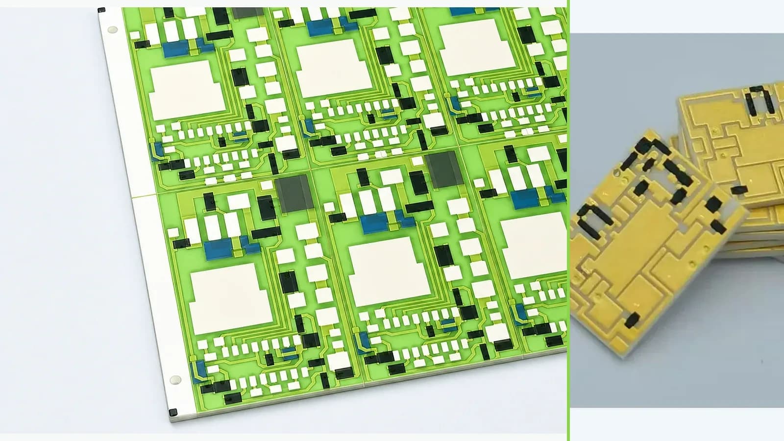
Printed thick film on ceramic and direct bonded copper, commonly abbreviated DBC, are different construction families rather than interchangeable labels for a ceramic PCB. Thick film forms selected conductors, resistors, dielectrics, crossovers, terminations, or other functional layers from compatible printable material systems that are processed on a ceramic surface. DBC bonds comparatively substantial copper foil to ceramic and then patterns that copper; its engineering value is usually considered where conductor cross-section, lateral heat spreading, power interconnection, or a solderable copper topology dominates. A choice cannot be made from ceramic thermal conductivity alone. The current path includes conductor geometry and interfaces; the thermal path includes device attach, metallization or copper, ceramic, baseplate, coolant or air, and contact resistances; reliability includes ceramic stress, copper or printed-layer behavior, corners, edges, vias or wraparounds, solder and wire bonds, cycling, isolation, contamination, and assembly. Feature density, embedded resistance, trim strategy, conductor loss, power cycling, flatness, attach area, procurement state, inspection, and evidence also matter. This page supplies a drawing-specific comparison method. It does not claim that ThickFilmPCB fabricates DBC, that either route is universally superior, or that the pictured printed AlN parts represent a DBC product.
Engineering review matrix
Each row links a design variable to evidence that can support a drawing or release decision.
| Variable | Control question | Verification route |
|---|---|---|
| Electrical mission | Specify DC, RMS, peak, pulse and fault current; working and transient voltage; duty, frequency, path loss, temperature coefficient, isolation, creepage and clearance at every node. | Calculate segment-level loss and field-sensitive geometry, then measure complete paths and isolation under the stated waveform and environment. |
| Thermal boundary | Define device heat map, simultaneous loads, allowable temperatures, ambient, baseplate or coolant temperature, convection, contact pressure, interface material, mounting, transient duration and instrumentation. | Correlate a stated thermal model with mapped temperatures and power using production-intent interfaces and calibrated sensors. |
| Ceramic construction | Name alumina, AlN or other authorized material, supplier grade, thickness, finish, flatness, bow, dimensions, edge quality, vias or holes, metallization compatibility, handling and incoming evidence. | Confirm purchase specification, supplier documents and incoming measurements; do not infer grade from color or a photograph. |
| Conductor architecture | For thick film, control paste family, fired thickness, line geometry, overlaps, refires and terminations; for DBC, control copper thickness, bond construction, etch profile, pattern balance, necks, edges and surface finish. | Cross-section and measure representative conductors, calculate resistance, inspect edges and compare electrical results with the released stack. |
| Interfaces and assembly | Define device attach, solder, braze, adhesive, wire or ribbon bond, terminals, plating, cleaning, rework, coating, baseplate and fixture sequence with compatible temperature histories. | Use joint-specific inspection, electrical and mechanical tests before and after representative assembly and conditioning. |
| Functional integration | List required printed resistors, dividers, sensors, heaters, dielectrics, crossovers, trim targets, discrete components, control loops and calibration, and assign each to a manufacturable layer or assembly. | Review schematic-to-artwork traceability and test every integrated function across tolerances and interactions. |
| Thermomechanical duty | Define assembly temperature excursions, ramp and dwell, power cycling, mechanical restraint, vibration, shock, mounting torque, copper or film pattern symmetry, local stress features and target life. | Use route-specific modeled strain screening and representative cycling with periodic electrical, thermal and microscopy evidence. |
| Evidence and supply | Control supplier, material and process revisions, approved sources, design-rule ownership, test methods, acceptance limits, traceability, alternates, lot strategy, change notification, volume and lifecycle. | Audit the released bill and traveler against the decision matrix and reopen qualification for any material, geometry, process or source change. |
Controlled model
Stack-level electrical and thermal comparison
Compare complete candidate stacks at identical boundary conditions. Use supplier-controlled material data for screening, measured geometry and interface data for prototypes, and application-level tests for release; do not turn a typical material property into a finished-assembly guarantee.
R_trace = ρL/(wt)First-order conductor resistance for length L, width w, thickness t, and effective resistivity ρ.
- Units
- Ω when dimensions and ρ use a consistent unit system
- Use boundary
- Printed-film thickness, fired microstructure, contacts, neck-downs and processing affect effective resistance; DBC copper thickness, etch geometry, temperature and joints also matter. Confirm on the actual path.
P_loss = I_rms²R_traceResistive heating generated in a conductor carrying RMS current.
- Units
- W
- Use boundary
- Does not include switching, spreading, contact, skin, proximity, terminal, via, wire-bond, solder or device losses. Use the mission current waveform and conductor temperature.
R_th,layer = t/(kA)One-dimensional through-plane thermal resistance of a uniform layer of thickness t, conductivity k, and heat-flow area A.
- Units
- K/W
- Use boundary
- A screening term only. Real assemblies have spreading, patterned metal, anisotropy, edge loss, interface resistance, voids, attach layers, baseplates and convection.
Δε_th ≈ (α_a − α_b)ΔTFirst-order differential thermal strain between two bonded materials over a temperature change.
- Units
- Dimensionless strain
- Use boundary
- Not a stress or fatigue-life prediction. Thickness, modulus, plasticity, creep, geometry, copper pattern, printed stack, process history and constraint must be modeled or tested.
Decision comparison
| Decision | Route A | Route B | Verification |
|---|---|---|---|
| Conductor cross-section and current path | Printed thick-film conductors can support compact routing and co-fired functional layers, but resistance depends on the named paste, fired thickness, geometry, terminations and process history. | Patterned DBC copper offers a different and generally much thicker conductor architecture, but current still concentrates at neck-downs, corners, interfaces, terminals and device attach. | Calculate each actual current path, map current density and loss at temperature, then test production-intent conductors, joints and cooling boundaries under the required waveform. |
| Thermal route | Printed ceramic can place resistive or sensing functions close to the substrate and may suit distributed heat or signal functions; printed metal alone is not a substitute for a complete heat-spreading analysis. | DBC copper can spread heat laterally and provide large attach areas, while the ceramic, copper pattern, solder, baseplate and interfaces still set junction-to-coolant performance and cycling stress. | Build a layer-by-layer thermal network, state heat-source footprint and boundary conditions, correlate with temperature measurements, and inspect attach quality. |
| Functional integration and patterning | Thick film can combine conductors with compatible printed resistors, dielectrics, crossover structures and trim features when the full material stack and sequence are qualified. | DBC emphasizes etched copper power topology; added sensing, resistance or insulation functions normally require separate structures, components, films or assembly steps. | Compare the released schematic, artwork, process stack, tolerance allocation, inspection accessibility, repair policy and assembly bill rather than only comparing line width. |
| Thermomechanical reliability | Printed layers introduce paste-to-ceramic and interlayer compatibility, refire, glass interaction, local thickness, trim and protection questions. | DBC introduces copper-to-ceramic stress, copper thickness and pattern balance, edge and corner geometry, ceramic type, attach area and power-cycling questions. | Use route-specific coupons and representative assemblies through mission-derived thermal and power cycling, followed by electrical measurement, microscopy and failure-plane classification. |
- Material thermal conductivity is only one term in a thermal path. Comparing a high-conductivity ceramic value with a complete substrate thermal resistance is dimensionally and physically misleading.
- A DBC design rule from one supplier and a thick-film TDS from one paste family are source-specific inputs. They are not portable process windows, finished-product specifications, or authorization to mix systems.
Failure controls
These are review prompts, not evidence that every risk applies or that every test is available.
- A
Calling every metallized ceramic DBC or assuming a printed ceramic photograph proves a bonded-copper construction
- B
Selecting from substrate conductivity alone while omitting copper or printed geometry, interfaces, spreading, attach, cooling and device heat map
- C
Assuming thick copper removes neck-down, joint, bond, terminal, isolation, temperature-rise or power-cycling constraints
- D
Assuming printed thick film provides an embedded function without a compatible named paste stack, process sequence, trim strategy and qualification
- E
Comparing supplier typical data obtained with different thicknesses, specimens, methods and boundary conditions as if it were finished-product performance
- F
Ignoring copper-pattern or printed-stack stress, ceramic edge condition, mounting constraint and assembly temperature history during reliability planning
- G
Publishing a DBC manufacturing, current, thermal, isolation or lifetime claim before route ownership and product-specific evidence are approved
Printed thick film versus DBC selection workflow
The order makes assumptions and ownership visible before a result is promoted to a requirement.
- 01
Freeze system requirements
Record circuit function, current and voltage waveforms, loss and temperature budgets, heat-source footprints, isolation, dimensions, mass, cooling, terminals, device attach, wire bonds, sensing, environmental mission, service life, standards, inspection, evidence, volume and change controls.
- 02
Define comparable route stacks
Name ceramic material, thickness and finish; printed conductor, resistor, dielectric and protection layers for thick film; copper thickness, bond construction and etch topology for DBC; plus attach, solder, wires, terminals, baseplate, coating and cooling for both.
- 03
Model electrical paths
Segment every conductor, neck-down, corner, pad, via or wraparound, bond, solder joint and terminal. Calculate resistance, current density, RMS loss and local temperature sensitivity under normal, transient, fault and imbalance conditions.
- 04
Model the thermal assembly
Map heat sources through metallization or copper, ceramic, attach, baseplate and coolant or air. Include lateral spreading, interfaces, void assumptions, contact pressure, edge losses, tolerances and the same boundary conditions for both candidates.
- 05
Review geometry and integration
Compare artwork rules, conductor thickness, isolation spacing, ceramic edge margin, pattern balance, device and bond pads, embedded resistor or sensor functions, trim access, inspection, singulation, handling, assembly sequence, rework and traceability.
- 06
Prototype each credible route
Build controlled coupons and production-intent assemblies from authorized source materials. Record actual geometry and processes; measure electrical, thermal, isolation, attach, surface and interface responses before and after assembly.
- 07
Stress, diagnose and decide
Apply mission-derived power, thermal, mechanical and environmental conditioning. Trend measurements, locate hot spots, classify failure planes, reconcile model error, supplier constraints, cost and supply risk, then approve one route, a partitioned architecture, or further work.
Reference boundary
Public method sources
These sources support the engineering method and terminology used in this technical guide. They do not establish a ThickFilmPCB material list, capability limit, customer result, certification, or finished-product specification.
- 01Rogers curamik ENDURANCE product information
Provides one DBC supplier's product-specific description, construction context and cycling-oriented claims under its stated conditions; it does not define all DBC, compare a ThickFilmPCB route, or guarantee an application.
- 02KYOCERA alumina material page
Provides supplier material-property context for named alumina grades and stated methods; typical ceramic data are screening inputs, not complete substrate or assembly performance.
- 03Heraeus C5729 gold thick-film conductor technical data sheet
Provides a named printable conductor's processing, fired-film and compatibility context under its supplier conditions; it neither represents every thick-film stack nor establishes a DBC comparison result.
Inputs for a practical review
Unknown values may be labelled unknown. The review should convert uncertainty into an explicit decision or validation task.
Send Drawings- 01
Schematic, netlist and mechanical drawings with envelope, ceramic outline, holes, edge zones, device positions, terminals, wire or ribbon bonds, solder areas, sensing and trim access
- 02
Normal, transient and fault current and voltage by path, duty, frequency, resistance or loss budget, isolation class, working altitude, pollution or coating state, creepage and clearance rules
- 03
Device heat-source maps, simultaneous power, allowable junction or substrate temperature, ambient, coolant or baseplate boundary, attach stack, interface material, mounting pressure and thermal-transient profile
- 04
Candidate ceramic material, grade, thickness, finish, conductivity evidence, flatness, bow, edge quality, vias or holes and approved suppliers
- 05
Printed-film candidate stack with named conductors, resistors, dielectrics, protection, firing or cure and refires; DBC candidate with copper thickness, bond construction, etch, finish and supplier design rules
- 06
Assembly sequence and materials for attach, solder, braze, adhesive, plating, wire bonds, terminals, cleaning, rework, coating, baseplate, fixture and cooling
- 07
Mission environment and validation: temperature range, thermal and power cycling, humidity, fluids, vibration, shock, pressure, duration, sample plan, measurements, failure criteria and analysis
- 08
Forecast volume, panel or substrate utilization, procurement state, approved-source and alternate policy, inspection and traceability records, change notification, cost horizon and responsible approvers