
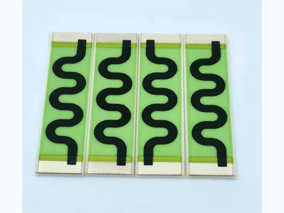
Overview
A high-voltage divider layout is an insulation-coordination and electric-field problem as well as a resistance-ratio problem. Creepage follows a surface path; clearance is the shortest air path; solid insulation, coatings, grooves, barriers, potting, housing, terminals, connectors, mounting hardware, contamination, condensation, altitude, overvoltage category, transient waveform, frequency, and applicable end-product standard can change the required design and test. Printed resistor length can distribute voltage, but conductor ends, trim cuts, corners, guards, pads, coating edges, voids, particles, substrate edges, solder joints, and nearby grounded or accessible metal create local fields that a simple V/d average does not reveal. Continuous dissipation and voltage coefficient can also shift the divider ratio, while faults can place unexpected voltage or power on one element. This guide does not publish universal spacing tables, because the governing edition, product category, working voltage, impulse, material, pollution, altitude, coating status, and construction must be selected by the responsible safety team. It claims no ThickFilmPCB voltage, spacing, isolation, coating, altitude, pollution, transient, power, TCR, ratio, or safety capability.
Failure controls
These are review prompts, not evidence that every risk applies or that every test is available.
- A
Copying a creepage or clearance number without the governing edition, voltage type, impulse, altitude, pollution, material, coating status, equipment category, and end-product context
- B
Measuring a two-dimensional board path while terminals, substrate thickness, fasteners, connectors, wires, housing, ground, and tolerances create a shorter three-dimensional path
- C
Treating average V/d as local electric field and missing stress at pad corners, trim cuts, voids, contamination, coating edges, substrate edges, or floating metal
- D
Reducing distance because a coating or potting is present without controlling material, thickness, cure, coverage, pinholes, voids, edges, repair, aging, and standard recognition
- E
Meeting divider ratio at low voltage while voltage coefficient, self-heating, load, leakage, transient distribution, TCR mismatch, drift, or faults change the result
- F
Publishing voltage or safety capability from a product photo or one dielectric test without design coordination, production tolerances, environmental evidence, and safety review
Engineering review matrix
Each row links a design variable to evidence that can support a drawing or release decision.
| Variable | Control question | Verification route |
|---|---|---|
| Governing safety framework | Define end-product standard and edition, jurisdiction, insulation function, protective means, accessible nodes, equipment category, overvoltage environment, pollution, altitude, and deviations. | Maintain a clause-traceable insulation-coordination record reviewed by the responsible safety authority. |
| Working and transient voltage | Specify DC, AC or mixed waveform, RMS, peak, frequency, common mode, impulse, switching transient, source impedance, energy, duration, repetition, startup, shutdown, and fault voltages. | Measure or derive from the reviewed system and apply appropriate voltage and transient tests with calibrated equipment. |
| Divider electrical performance | Set element values, ratio, load, leakage, TCR and tracking, voltage coefficient, self-heating, tolerance, trim, calibration, bandwidth, capacitance, stability, and error budget. | Measure individual elements and loaded transfer across voltage, temperature, time, frequency and environmental states. |
| Creepage and clearance geometry | Define three-dimensional paths among all potentials, ceramic surfaces, edges, holes, slots, grooves, barriers, terminals, mounting, connector, housing, ground, and accessible metal with tolerance. | Inspect and measure the assembled construction against drawing datums and the selected standard's path rules. |
| Surface material and contamination | Identify substrate and protection materials, applicable material classification, roughness, cleanliness, dust, humidity, condensation, fluids, residues, migration, tracking, and maintenance state. | Use controlled material evidence, cleanliness and environmental conditioning, biased tests, and post-test inspection as required. |
| Coating, potting, or barrier | Specify product, thickness, coverage, cure, adhesion, compatibility, edges, keep-outs, pinholes, bubbles, voids, repair, inspection, aging, and whether the governing standard recognizes the treatment. | Qualify the production process and inspect or section tolerance-condition samples before and after environmental and electrical tests. |
| Local field and thermal stress | Review conductor corners, trim cuts, pads, gaps, guards, floating metal, parasitic capacitance, resistor power, gradients, substrate and coating interfaces, and nearby heat. | Correlate field and thermal models with voltage, temperature, leakage, transient and damage evidence on production-intent assemblies. |
| High-voltage test and safety | Define dielectric, impulse, leakage, insulation, partial-discharge or other applicable methods, energy limits, ramp, dwell, discharge, interlock, fixture, environment, sampling, acceptance, and post-test handling. | Use calibrated equipment, controlled personnel procedures, raw traces, failure classification, uncertainty, and drawing-linked records. |
Controlled model
Divider transfer, distributed voltage, and insulation model
Separate functional divider accuracy from protective insulation compliance. Calculate node voltages and resistor loading for nominal and fault states, then review electric-field concentration and determine creepage, clearance, solid-insulation, coating, and test requirements from the applicable current standard and end product.
K = V_out/V_in = R_low/(R_high + R_low)Ideal unloaded transfer of a two-element divider measured across the lower resistor.
- Units
- K dimensionless; V in V; R in Ω
- Use boundary
- Assumes negligible source and load impedance, no leakage, no parasitics, no temperature or voltage coefficient, and intact components. Use the complete network for final analysis.
R_low,L = R_low ∥ R_load; K_L = R_low,L/(R_high + R_low,L)Loaded divider transfer with a finite measurement or control input impedance.
- Units
- Resistances in Ω; K_L dimensionless
- Use boundary
- Add source impedance, input protection, capacitance, leakage, frequency, common-mode behavior, tolerances, and faults where material.
V_i = V_in R_i/ΣR; P_i = V_i²/R_iIdeal DC voltage share and power in each series resistor element.
- Units
- V_i in V; P_i in W; R_i in Ω
- Use boundary
- Resistance can depend on voltage, temperature, self-heating, tolerance, aging, and failure. Transient distribution also depends on capacitance and field geometry.
E_avg = ΔV/dAverage field over a stated straight distance used only for preliminary screening.
- Units
- V/mm or V/m
- Use boundary
- Not a local peak and not a spacing rule. Edges, corners, conductors, voids, material interfaces, contamination, pressure, humidity, altitude, frequency, transients, and geometry require appropriate field analysis and standards.
ΔK/K ≈ (1−K)(δR_low/R_low − δR_high/R_high)First-order divider transfer sensitivity to differential fractional resistance change.
- Units
- Dimensionless, commonly % or ppm
- Use boundary
- Small-error unloaded approximation. Include covariance, load, leakage, voltage coefficient, thermal gradient, trim, measurement uncertainty, and aging separately.
Decision comparison
| Decision | Route A | Route B | Verification |
|---|---|---|---|
| Creepage versus clearance | Creepage is measured along an insulating surface and depends on surface material classification, pollution, moisture and contamination, geometry, tracking behavior, coating treatment, and the selected standard. | Clearance is measured through air and depends on impulse or transient stress, working voltage as applicable, altitude, field shape, overvoltage environment, and the selected standard. | Create separate annotated paths on the complete 3D assembly and have the responsible safety reviewer apply the current governing clauses and tests. |
| Bare versus coated or potted construction | Bare ceramic and conductors allow direct inspection but remain exposed to contamination, humidity, condensation, particles, and accessible surface paths. | Coating or potting may change the insulation treatment only when material, coverage, adhesion, thickness, cure, pinholes, edges, voids, compatibility, aging, repair, and applicable standard conditions are controlled. | Qualify the production coating or potting process and inspect deliberate openings, edges, bubbles and hidden regions; do not reduce spacing from a coating name alone. |
| One long resistor versus series segmentation | One printed element simplifies nodes but concentrates the full voltage and relies on its continuous geometry, material, trim, protection, and local field control. | Series elements can distribute voltage and power, provide intermediate grading or diagnostics, and alter fault response, but add pads, gaps, parasitic capacitance, tolerance, joints, area, and failure modes. | Analyze steady, transient, tolerance and single-fault states and validate the production-intent network and insulation architecture. |
| Geometric spacing versus field grading | Longer distance can reduce average field but may not remove high local stress at sharp pads, trim ends, contamination paths, substrate edges, or nearby metal. | Guarding, rounded geometry, controlled potential grading, shields, barriers, or encapsulation can manage local fields but introduce their own leakage, parasitic, process, inspection, and fault boundaries. | Use reviewed electrostatic or transient analysis and high-voltage tests on tolerance-condition assemblies under relevant environments. |
- Do not measure creepage and clearance only in a 2D artwork file; terminal height, substrate thickness, coating edge, fastener, enclosure, wire, connector, and assembly tolerances create three-dimensional paths.
- High-voltage testing can be destructive or hazardous and does not replace design coordination. Define energy limiting, interlocks, discharge, fixture, instrumentation, personnel controls, and post-test handling.
High-voltage divider layout workflow
The order makes assumptions and ownership visible before a result is promoted to a requirement.
- 01
Establish the safety basis
Name the end-product, governing standards and editions, jurisdiction, working voltage, impulse and other transients, source impedance and energy, frequency, altitude, pollution, environment, accessible parts, insulation role, protective means, and single-fault assumptions.
- 02
Define divider accuracy and loading
Specify ratio, absolute values, source and load, input protection, bandwidth, capacitance, leakage, TCR and tracking, voltage coefficient, self-heating, trim, calibration, measurement uncertainty, stability, and allowed error through nominal and fault states.
- 03
Allocate voltage and power
Choose element segmentation, nominal and tolerance voltage sharing, power, pulse, gradients, current, pads, terminals, conductor widths, trace length, trim location, and thermal path. Analyze open, short, drift, contamination and load faults without assuming equal sharing.
- 04
Map every insulation path
Annotate creepage, clearance, solid insulation, edges, holes, slots, grooves, barriers, coatings, potting, connector, solder, wires, mounting, housing, ground, accessible metal, contamination paths, and assembly tolerance in three dimensions.
- 05
Review local electric fields
Identify sharp corners, conductor ends, trim cuts, voids, protection edges, necks, high-gradient gaps, dielectric interfaces, floating metal, guard transitions, and parasitic capacitance. Use rounded geometry, grading, shielding, barriers, or spacing only within a reviewed system.
- 06
Apply standards and process controls
Record the exact clauses, tables, correction factors, material classification, coating or potting status, required tests, manufacturing tolerances, cleanliness, cure, coverage, inspection, repair, sampling, and deviations selected by the responsible safety team.
- 07
Validate the production assembly
Test electrical transfer, resistance, temperature, leakage, insulation, transient response, environmental condition, and single faults with safe fixtures and uncertainty. Inspect for tracking, flashover, damage, drift, contamination, voids, cracks, and protection defects before release.
Reference boundary
Public method sources
These sources support the engineering method and terminology used in this technical guide. They do not establish a ThickFilmPCB material list, capability limit, customer result, certification, or finished-product specification.
- 01IEC 60664-1:2020 — Insulation coordination principles
Supports the principles, requirements, tests, altitude guidance, creepage, clearance, and solid-insulation scope for equipment within the standard's stated voltage and frequency boundary; exact application requires the licensed standard and end-product requirements.
- 02IEC 60664-3:2016 — Coating, potting or moulding protection
Supports treating coating, potting and moulding as controlled insulation constructions with design and test conditions rather than as automatic permission to reduce distance; exact clauses require the licensed standard.
- 03Heraeus R8900 Series thick-film resistor TDS
Supports the material boundary that voltage coefficient, standard working voltage, overload, power, geometry, substrate, firing and trim data are specific to a named resistor system and test construction; values do not establish a divider rating.
Inputs for a practical review
Unknown values may be labelled unknown. The review should convert uncertainty into an explicit decision or validation task.
Send Drawings- 01
System schematic with every high-voltage, low-voltage, ground, shield, accessible and floating node, divider values, load, protection, isolation boundary, and fault states
- 02
Working DC or AC voltage, RMS and peak, frequency, impulse and switching transients, source impedance and energy, repetition, startup, shutdown, altitude, pollution, and environment
- 03
Applicable end-product standards and editions, jurisdiction, equipment category, overvoltage context, insulation class, protective means, material classification, clauses, and deviations
- 04
Complete 3D assembly drawing with ceramic, conductors, resistors, trim, pads, coating or potting, edges, holes, slots, barriers, connector, wires, mounting, housing, ground, and tolerances
- 05
Ratio, load, tolerance, TCR and tracking, voltage coefficient, power, pulse, thermal boundary, leakage, bandwidth, parasitics, calibration, stability, and measurement uncertainty
- 06
Substrate and printed stack, protection material and process, cleanliness, cure, coverage, inspection, repair, assembly, rework, contamination, humidity, condensation, and fluids
- 07
Prototype quantity, field and thermal analysis, electrical and environmental test matrix, safe fixture, sampling, acceptance, reports, responsible safety reviewer, and change control