
On this page
- Start with the Pattern-Formation Method
- Separate Precision from Stability
- Match Conductor Construction to Current and Joining
- Compare the Complete Cost Structure
- Use a Decision Matrix, Not a Slogan
- A Worked Engineering Review
- Design Review Checklist
- Questions Engineers Commonly Ask
- Related Engineering Resources
- Closing Note
Prepared by Chipsimple Engineering Team, Engineering and technical content review
Published online August 10, 2026 · Reviewed August 10, 2026
ENGINEERING ARTICLE 01 / VOLUME 1
Thick Film vs. Thin Film Ceramic Circuits: A Process-Based Selection Guide
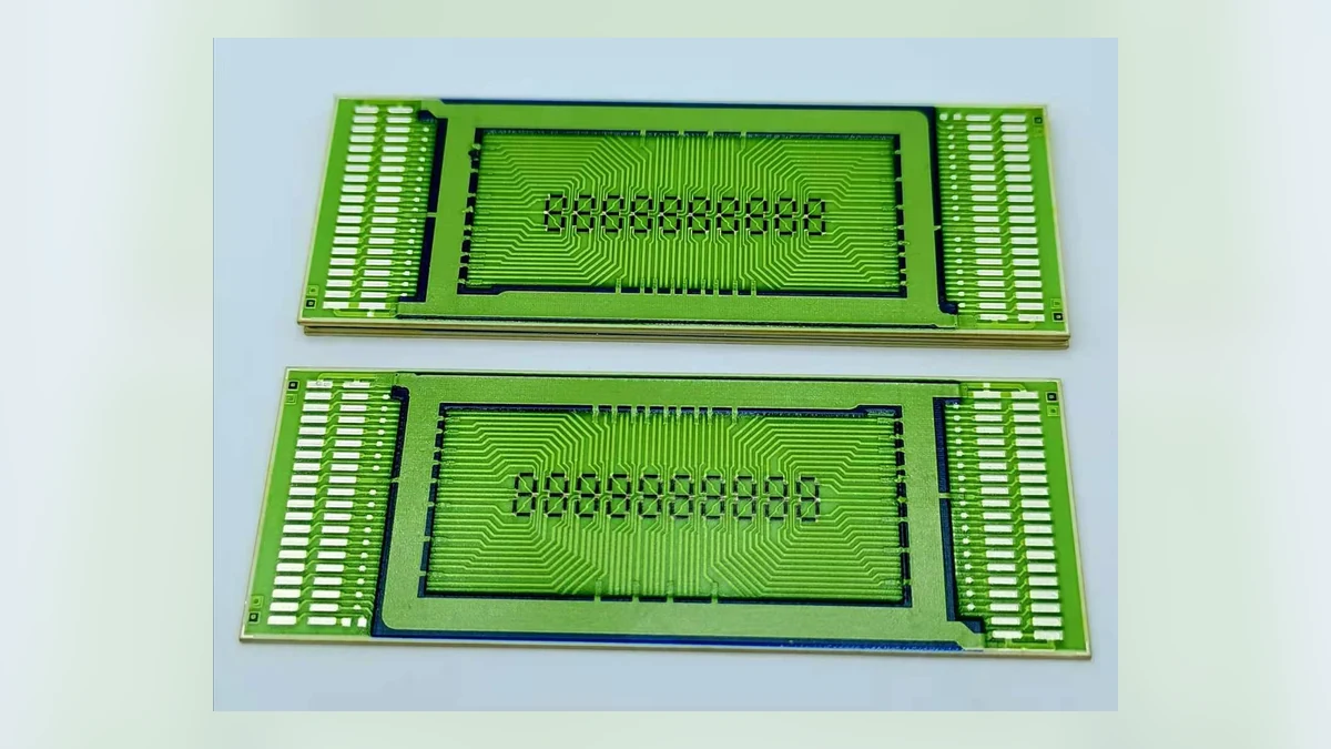
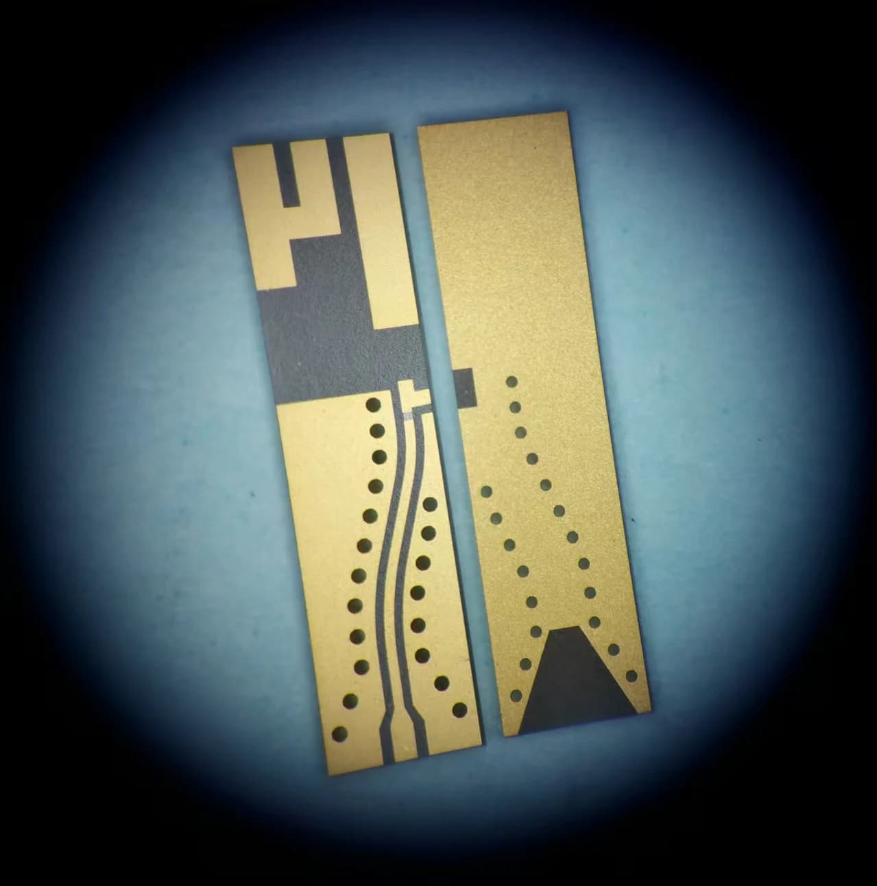
For a buyer, the two technologies are often presented as alternatives. For a process engineer, they are different manufacturing chains. Thick film normally prints formulated pastes and consolidates them through drying and firing. Thin film begins with a deposited layer and commonly uses photolithography and etching to define the pattern. That distinction shapes almost every downstream decision: conductor thickness, minimum geometry, achievable resistor range, trimming strategy, tooling cost, inspection method and repair options.

Start with the Pattern-Formation Method
Thick film transfers a paste through a patterned screen, while thin film defines a deposited coating by subtractive or lift-off processing. The consequence is practical: printed geometry is influenced by mesh, emulsion, paste rheology and firing shrinkage, whereas thin-film geometry is dominated by deposition and photolithographic control. This is one reason thick film vs thin film ceramic circuit cannot be reduced to a single catalogue value.
During design review, state the functional minimum line, spacing and registration requirement and allow the supplier to map it to a qualified route. The objective is not to freeze every process setting on the customer drawing, but to define the functional boundary that the manufacturer must protect.
A useful evidence package contains layer artwork, coupon measurements and magnified edge inspection from a representative lot. Comparing those records with the approved construction is more informative than judging an isolated photograph or one resistance reading.
Watch for using a thin-film drawing convention for a printed paste and discovering rounded corners, neck-down or insufficient spacing after firing. It often indicates that two individually acceptable variables have combined at the edge of their windows.
Separate Precision from Stability
A tight initial resistance is not the same as a stable resistance over temperature, time and assembly. Consequently, thin films can support fine geometry and low trimming increments, while thick films can offer robust fired structures and wide resistance choices when the paste and geometry are correctly matched. The engineering value comes from understanding the direction and sensitivity of the effect, not from memorising a nominal number.
A robust drawing or process plan will build separate limits for as-fired value, post-trim value, temperature coefficient and permitted drift after thermal exposure. This makes the design intent visible and gives the supplier room to use a qualified material set without changing the function.
The result can be checked through resistance data before trimming, after trimming and after the agreed stabilisation or assembly simulation. Where possible, keep readings before and after the next thermal or mechanical operation; the delta often reveals more than the final value.
The failure pattern to investigate is accepting a precise room-temperature value that later moves outside the circuit error budget. Before changing materials, confirm orientation, lot history, measurement method and acceptance limits.
Match Conductor Construction to Current and Joining
The physical starting point is straightforward: Conductor thickness and metallurgy determine more than DC resistance. From there, current density, pad erosion, solder leaching, wire-bond compatibility and high-temperature ageing may favour different material systems. For thick film vs thin film ceramic circuit, the important issue is the amount of process margin left after normal variation is included.
On the drawing and in the review record, identify how each pad will be joined and which areas carry pulse, continuous or sense current. Keep the requirement functional wherever possible, while making any safety- or interface-critical boundary unambiguous.
A production trial should capture fired thickness or sheet resistance data, adhesion tests and a joining trial using the intended assembly process. Record the condition of the specimen and the next operation so that a later change can be traced to a specific stage.
If the team sees choosing the circuit technology from line width alone while overlooking a pad or termination failure, pause before adding inspection or rework. First check whether the layout and the qualified process window are asking for contradictory outcomes.
Compare the Complete Cost Structure
In a stable manufacturing route, unit price depends on tooling, masks or screens, process steps, yield and inspection rather than substrate area alone. This means a process with lower initial tooling can be attractive for prototypes, while a higher-control route may pay back when fine geometry or repeatability drives yield. The observation is especially useful because it connects a visible feature to an electrical, thermal or mechanical consequence.
The control plan should quote the realistic volume stages and ask which tooling is reusable after a design revision. It should also name the drawing characteristic or coupon that represents the requirement, avoiding an instruction that depends on personal interpretation.
Evidence comes from a cost breakdown that distinguishes engineering, tooling, recurring production and test coverage. A trend across position or lot is usually more valuable than a perfect reading from one hand-picked sample.
Investigate optimising the first prototype price and paying for repeated redesign or excessive inspection in production. The pattern may identify a narrow process interaction long before the final circuit becomes an open, short or out-of-tolerance value.
Use a Decision Matrix, Not a Slogan
A useful way to frame the decision is this: Neither technology is universally more advanced. As a result, the best process is the one whose normal capability window surrounds the electrical, mechanical and commercial requirements with margin. That cause-and-effect chain should remain visible when thick film vs thin film ceramic circuit is reviewed with purchasing and quality teams.
The manufacturing boundary is protected when the team can rank feature size, resistance precision, power handling, joining method, environment, volume and lifecycle importance. This approach separates the customer's functional need from the supplier's machine-specific compensation.
Confirm the decision with a documented design review showing why the chosen process owns the critical characteristics. Include both typical and boundary-condition specimens where the failure consequence justifies them.
The symptom selecting a technology because of a generic statement such as higher precision, lower cost or better reliability deserves a structured investigation. Check material lot, artwork position, thermal history and measurement setup before assigning a single cause.
A Worked Engineering Review
Consider a ceramic control module with printed resistors, several wire-bond pads and a compact signal network. If the dominant requirement is fine interconnect geometry and very small resistance adjustments, a thin-film route may be attractive. If the design needs a broader printed-resistor range, thicker current paths and an economical screen-based build, thick film may be the stronger starting point. The engineer should then test the boundary conditions: Can the intended pad metal survive the joining process? Is laser-trim access available? Does the resistor TCR fit the system budget? Are the line and space values normal capability or exceptional capability? The answer is produced by this sequence of questions, not by the ceramic outline itself.
Design Review Checklist
- Define minimum line, spacing and registration by function.
- Separate initial resistance tolerance from TCR and drift.
- Identify solder, braze, wire-bond or adhesive interfaces.
- Provide prototype, pilot and annual volume assumptions.
- Agree the inspection and qualification evidence before tooling release.
Questions Engineers Commonly Ask
Is thin film always more accurate?
Thin film commonly supports finer geometry and small trimming increments, but system accuracy also depends on TCR, thermal gradients, contact resistance, assembly stress and the measurement method. Accuracy should be allocated across the complete circuit rather than inferred from the process name.
Can thick film make precision resistor networks?
Yes, when the resistor paste, geometry, firing control, trim strategy and stabilisation are designed as one system. The achievable tolerance and tracking requirement must be reviewed with the actual resistance range and layout.
Should both technologies be quoted for a new design?
It is useful when the design sits near a process boundary. Give both suppliers the same functional specification and compare the proposed construction, risks, tooling, test plan and lifecycle cost—not only the headline price.
Related Engineering Resources
Closing Note
A good technology selection leaves fewer surprises in later drawings. Once the process route is chosen, update the layout rules, material notes, acceptance plan and assembly method so that the decision remains visible to every team that touches the product.