
Overview
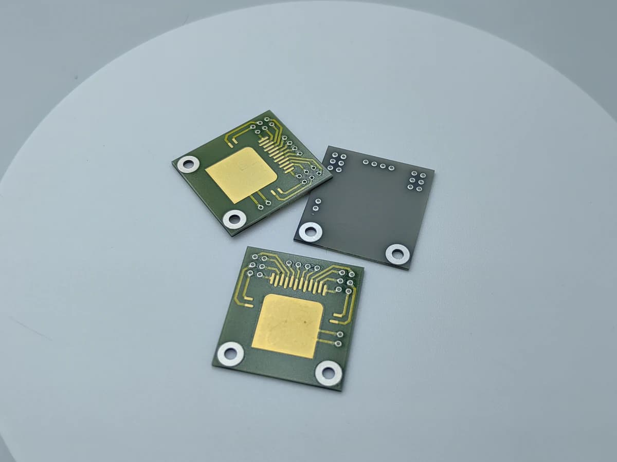
A wire-bond pad on a thick-film ceramic circuit is an engineered interface among substrate, fired conductor, optional finish, neighboring dielectric or overglaze, die placement, wire metallurgy and diameter, bond process, tool access, fixture support, cleaning, handling, and the assembly environment. A large gold-colored rectangle is not automatically bondable. Surface composition, roughness, thickness, glass content, contamination, oxidation or other change, probe marks, refires, dielectric encroachment, pad support, and prior thermal history can alter bond formation and failure mode. Pad dimensions must also support the chosen ball, wedge, ribbon, or other approved process, positional tolerance, tool footprint, deformation, pull or shear access, loop geometry, current path, rework policy, and edge clearance. Gold and aluminum wire, thermosonic ball and ultrasonic wedge methods, and thin- versus thick-wire processes are not interchangeable labels; each needs compatible metallurgy, equipment, parameters, fixture, and acceptance. This guide creates a drawing-led review and qualification plan. It does not claim a ThickFilmPCB pad finish, minimum size, wire type, bond window, pull or shear strength, rework count, yield, temperature, or life result.
Failure controls
These are review prompts, not evidence that every risk applies or that every test is available.
- A
Treating a gold-colored pad as proof of gold chemistry, compatible surface, wire bondability, fired thickness, or pad adhesion
- B
Copying a minimum pad size without the actual wire, tool, bond deformation, placement tolerance, access, edge clearance, support, and rework policy
- C
Optimizing average pull or shear while the failure distribution includes pad lift, ceramic fracture, heel damage, or censored fixture results
- D
Probing, touching, storing, cleaning, refiring, or coating a bond region without controlling surface age, contamination, marks, and dielectric encroachment
- E
Transferring parameters among gold and aluminum wire, ball and wedge, thin and thick wire, different tools, or different pad metallurgies
- F
Releasing an initial bond without thermal, humidity, vibration, shock, electrical, encapsulation, assembly, and change-control evidence
Controlled model
Bond-pad interface and load-path model
Separate electrical path, local bond contact, pad-to-ceramic adhesion, wire deformation, loop mechanics, and test fixture. The same measured pull force can represent wire break, neck failure, interfacial lift, pad lift, ceramic fracture, or fixture limitation, so failure mode is part of the result.
R_path = R_wire + R_bond,1 + R_pad + R_bond,2 + R_returnBreaks the bonded interconnect into wire, bond, pad, second connection, and return-path contributions.
- Units
- All terms in Ω
- Use boundary
- Small terms require a defined Kelvin or other method, stable temperature, contact arrangement, and uncertainty. Continuity alone does not prove mechanical or environmental integrity.
J_wire = I/A_wire = 4I/(πd²)Nominal current density in a round wire of diameter d.
- Units
- A/m² or A/mm²
- Use boundary
- Does not set allowable current or temperature. Bond neck, heel, loop length, pulse, duty, convection, pad spreading, adjacent wires, and fault current require separate analysis and test.
σ_app = F_shear/A_bond; f_norm = F_pull/dTwo possible normalized reporting quantities for a defined shear footprint or wire diameter.
- Units
- σ in N/mm²; f_norm in N/mm when matching units are used
- Use boundary
- Use only within the same wire, bond, tool, geometry, loading direction, speed, fixture, and standard. Normalization cannot make unlike ball, wedge, ribbon, or pad-lift tests equivalent.
ΔL_free ≈ α_wire L_loop ΔTFirst-order free thermal expansion of the wire loop over a uniform temperature change.
- Units
- ΔL and L in the same length unit; α in 1/K; ΔT in K
- Use boundary
- Real loop stress depends on shape, anchors, substrate and die movement, gradients, creep, encapsulation, vibration, and plastic deformation; use mechanical analysis and cycling tests.
Decision comparison
| Decision | Route A | Route B | Verification |
|---|---|---|---|
| Ball versus wedge bonding | A ball-bond process commonly uses a capillary, free-air ball, specific wire, pad access, ultrasonic and thermal settings, and loop sequence. | A wedge-bond process uses a wedge tool, wire or ribbon, directional access, first and second bond geometry, and a different deformation and loop strategy. | Freeze the actual equipment, tool, wire, pad and package geometry, then qualify its parameter window and failure distribution; do not derive pad rules from the other process. |
| Gold versus aluminum wire | Gold wire requires compatible pad metallurgy and review of contamination, intermetallic or galvanic interfaces, process temperature, cost, and environment. | Aluminum wire requires its own pad compatibility, oxide disruption, ultrasonic process, tool, deformation, corrosion, and dissimilar-metal review. | Use supplier and process-owner documentation for the exact wire and pad, then validate joints and conditioned assemblies with failure analysis. |
| Bond formation versus pad adhesion | A visually acceptable wire-to-pad bond can still transfer load into a weak fired-pad-to-ceramic interface. | A strongly adhered pad may still form a weak, contaminated, overworked, underworked, or geometrically incomplete wire bond. | Classify failure at the wire, neck, heel, bond interface, pad film, pad-to-substrate interface, ceramic, and fixture rather than reporting force alone. |
- Preserve separate probe and bond regions when electrical probing can mark, contaminate, harden, or otherwise change the production bond surface.
- A pull or shear acceptance must name the applicable method, wire and bond type, sample preparation, destructive or nondestructive intent, failure codes, and treatment of censored results.
Wire-bond pad design workflow
The order makes assumptions and ownership visible before a result is promoted to a requirement.
- 01
Define the bonded interconnect
State signal or power function, current, voltage, pulse, duty, wire count, redundancy, die or terminal nodes, allowable drop, loop envelope, package and assembly sequence, environment, inspection, rework, and failure consequence.
- 02
Lock pad and substrate materials
Name ceramic grade and surface, fired conductor or finish, compatible dielectrics and overglaze, firing and refire history, cleaning, storage, handling, probe exposure, and pad-to-substrate evidence. Color or a generic gold label is insufficient.
- 03
Select wire and bond process
Define wire or ribbon alloy, coating, diameter or cross-section, temper, spool and shelf controls, ball or wedge route, tool, equipment, ultrasonic mode, force, time, stage temperature, atmosphere, sequence, and process-owner documentation.
- 04
Design pad, access, and support
Allocate pad length and width, tolerances, bond footprint, placement, tool approach, conductor neck, dielectric and edge clearance, die and wire spacing, probe keep-out, pull or shear access, substrate support, flatness, fixture, and rework area.
- 05
Develop a controlled process window
Use production-intent coupons and lots to vary only reviewed parameters. Record tool condition, alignment, surface age and cleanliness, force, energy, time, temperature, deformation, continuity, resistance, visual condition, and immediate mechanical failure distribution.
- 06
Classify and investigate failures
Separate wire break, neck or heel failure, bond separation, pad cohesive fracture, pad lift, ceramic fracture, dielectric damage, loop collision, and fixture limitation. Use microscopy or other agreed analysis and retain individual data, not only averages.
- 07
Condition and release
Test production assemblies through thermal cycling, humidity, vibration, shock, electrical load, storage, encapsulation or coating, and other relevant exposures. Link the approved stack, wire, tool, process version, fixture, test method, records, and change triggers to the drawing.
Engineering review matrix
Each row links a design variable to evidence that can support a drawing or release decision.
| Variable | Control question | Verification route |
|---|---|---|
| Pad metallurgy and fired surface | Specify paste or finish code, fired thickness, substrate, refires, overglaze clearance, surface age, roughness or condition, cleaning, storage, and probe history. | Review material and traveler records, inspect unbonded surfaces, and correlate lots with bond and pad-interface failure data. |
| Pad geometry and tolerance | Define bondable area, artwork and fired dimensions, edge and dielectric clearance, conductor neck, tool and wire footprint, placement tolerance, probe keep-out, and rework region. | Measure production pads and overlay bond deformation and placement against drawing datums and worst-case stack-up. |
| Wire or ribbon | Name alloy, coating, diameter or section, temper, elongation or other controlled supplier properties, spool, storage, handling, shelf, and lot traceability. | Use supplier certificates and incoming or process checks agreed for the application; do not substitute metallurgy or size without review. |
| Bond tool and parameters | Control equipment, capillary or wedge part and wear, force, ultrasonic energy or power, frequency mode, time, stage temperature, atmosphere, sequence, alignment, and maintenance. | Record parameter and tool identity for coupons and production samples and monitor mechanical and visual distributions. |
| Substrate support and flatness | Define fixture support under the pad, vacuum or clamp, substrate thickness and bow, nearby cavities or edges, die attach, and assembly compliance. | Inspect fixture contact and compare bond response at nominal and tolerance support states without forcing brittle ceramic. |
| Loop and mechanical envelope | Set first and second bond locations, loop height and length, heel, clearance, sweep, resonance, thermal expansion, encapsulation, wire crossing, and external loads. | Measure loops and condition assemblies through relevant thermal, vibration, shock, and handling sequences. |
| Electrical loading and heat | Define current, voltage, pulse, duty, parallel sharing, wire and bond resistance, acceptable drop, local heat path, ambient, and fault current. | Measure complete path resistance, voltage, current, and temperature under nominal, tolerance, transient, and fault conditions. |
| Test and failure classification | Name visual, pull, shear, electrical, microscopy, conditioning, sample, rate, direction, fixture, failure code, acceptance, uncertainty, and censoring rules. | Calibrate the method, retain individual results and images, and trend force and failure distribution by lot, tool, pad, and process state. |
Reference boundary
Public method sources
These sources support the engineering method and terminology used in this technical guide. They do not establish a ThickFilmPCB material list, capability limit, customer result, certification, or finished-product specification.
- 01DuPont 5771 Gold Conductor technical data sheet
Supports the dependency of one fired gold conductor's published bond behavior on alumina substrate, print and fired thickness, profile, compatible dielectric, specific wire, bonder, tool, stage temperature, and test setup; it does not qualify another process.
- 02NASA — Quality control of microelectronic wire bonds
Supports treating ultrasonic wire bonds to thin- and thick-film gold on ceramic as a controlled inspection and test problem with failure-location evidence; the historical report supplies no current ThickFilmPCB requirement or capability.
- 03NASA — Body of Knowledge for Copper Wire Bonds
Supports the broader boundary that wire metallurgy, pad interface, corrosion, cracking, delamination, package environment, and failure mechanisms must be reviewed together; copper-specific findings are not transferred to gold or aluminum wire.
Inputs for a practical review
Unknown values may be labelled unknown. The review should convert uncertainty into an explicit decision or validation task.
Send Drawings- 01
Assembly and circuit drawings with die and terminal nodes, pad locations and datums, bondable area, tolerances, edge and dielectric clearance, tool access, loop envelope, and probe keep-outs
- 02
Ceramic substrate and pad material codes, surface or finish, fired thickness, conductor and dielectric stack, firing and refire history, cleaning, storage, and allowed substitutions
- 03
Wire or ribbon alloy, coating, diameter or cross-section, ball or wedge method, equipment, tool, stage temperature, force, ultrasonic settings, time, sequence, and spool controls
- 04
Current, voltage, pulse, duty, allowable resistance and drop, parallel paths, local thermal boundary, ambient, fault current, ground, and isolation requirements
- 05
Substrate support, flatness, fixture, die attach, loop length and height, clearance, encapsulation or coating, connector, mechanical loads, and rework policy
- 06
Temperature, humidity, condensation, corrosion, vibration, shock, storage, bias, power cycling, assembly handling, and other conditioning requirements
- 07
Visual, pull, shear, electrical and microscopy methods, sample plan, acceptance and failure codes, uncertainty, traceability, report, reviewer, and change-control requirements