
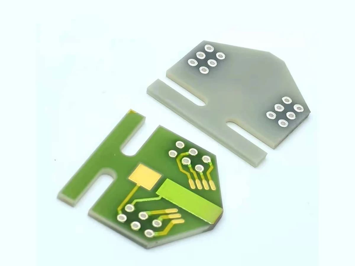
Overview
A thermal via is useful only as part of a defined heat path from a source, through the ceramic and via structure, into a spreader, mount, fluid, or ambient boundary. Hole diameter, pitch, array footprint, wall metallization or fill, material conductivity, porosity, surface pads, dielectric layers, interface pressure, and substrate stress all influence the result. A dense array can reduce one modeled resistance while consuming routing area, concentrating process risk, or weakening a brittle region. Thermal and electrical via functions must also be separated: a structure intended to conduct heat may be electrically active, grounded, isolated, or floating, and each choice changes layout and validation.
Engineering review matrix
Each row links a design variable to evidence that can support a drawing or release decision.
| Variable | Control question | Verification route |
|---|---|---|
| Heat source and footprint | Define location, area, dissipation waveform, contact layer, allowable source and ceramic temperatures, neighboring sources, and transient states. | Measure synchronized electrical input and temperatures at drawing-referenced source and surrounding locations. |
| Via construction | Specify hole process and profile, wall metallization or fill, materials, fired thickness or density observations, pads, firing sequence, refires, and surface finish. | Inspect sections or other justified construction evidence across representative positions and correlate with continuity and thermal results. |
| Array geometry | Set diameter, pitch, rows, footprint, edge distance, pad overlap, registration, keep-outs, source coverage, and nominal/tolerance cases. | Measure critical fired features and compare array position and defects with thermal-map residuals. |
| Ceramic and printed stack | Name substrate material, thickness, conductivity source, dielectric, conductor, resistor, protection, holes, edges, and print/fire history. | Retain controlled material identity and inspect flatness, cracks, layers, and via interfaces after complete processing. |
| Sink and interfaces | Define spreader or housing material, contact area, interface material and thickness, pressure, fasteners, flatness, insulation, airflow or fluid, and ambient. | Characterize or bound contact behavior and repeat correlation at nominal and degraded interface conditions. |
| Electrical boundary | Identify every via potential, ground, current, fault, accessible metal, isolation layer, creepage path, working/transient voltage, and contamination assumption. | Use net review plus project-selected continuity, resistance, leakage, and withstand methods on the assembled stack. |
| Stress and lifecycle | Include removed ceramic area, hole spacing, edge proximity, clamp load, CTE mismatch, cycling, vibration, assembly, humidity, and allowable change. | Inspect for cracks, delamination, via damage, flatness change, and thermal/electrical shift before and after representative exposures. |
Controlled model
Parallel heat-path and spreading model
A via is not a standalone thermal resistor. Screen the axial via contribution and the ceramic path, then add constriction, spreading, pad, interface, source, sink, and contact effects. Use effective properties only when the array scale and assumptions are stated. Correlate the model to sectioned construction and temperature measurements on a production-intent assembly.
θ_via ≈ L / (k_v A_v)First-pass axial thermal resistance of one uniform via material path.
- Units
- θ in K/W; L in m; k in W/(m·K); A in m²
- Use boundary
- Assumes uniform solid material and one-dimensional conduction. Plated walls, partial fill, porosity, contacts, taper, voids, and spreading require an adjusted model.
1/θ_array ≈ Σ(1/θ_i)Combines ideal parallel thermal paths for multiple vias or materials.
- Units
- θ in K/W
- Use boundary
- Only for paths sharing appropriate source and sink temperatures. Mutual spreading, edge effects, nonuniform source flux, and unequal interfaces limit independence.
θ_layer = t/(kA)Screens conduction through a uniform ceramic, pad, dielectric, or interface layer.
- Units
- K/W
- Use boundary
- Does not capture contact resistance, lateral spreading, anisotropy, temperature dependence, local pads, or changing assembly pressure.
Decision comparison
| Decision | Route A | Route B | Verification |
|---|---|---|---|
| Metallized-wall via versus filled via concept | A wall-metallized hole creates an annular path whose effective area depends on actual wall coverage, thickness, continuity, and interfaces. | A filled concept may increase path area but adds fill chemistry, shrinkage, void, firing, flatness, surface termination, and compatibility controls. | Section representative vias, identify materials and defects, and correlate geometry with measured thermal and electrical behavior; do not infer fill from an exterior photograph. |
| Few large vias versus many small vias | Larger holes can offer path area and easier inspection but remove more ceramic and routing space and can raise local stress or pad demands. | Smaller dense arrays distribute paths but increase registration, coverage, blockage, inspection, mutual-spreading, and process-yield concerns. | Compare nominal and tolerance arrays in the same source/sink assembly using section evidence, temperature maps, mechanical inspection, and relevant cycling. |
| Electrically connected versus isolated heat path | A conductive via tied to a node or ground can share electrical and thermal roles but requires current, potential, return-path, and fault review. | An isolated thermal structure avoids intentional node connection but still needs clear dielectric boundaries, spacing, contamination control, and accessible-metal analysis. | Review the complete electrical net and section, then apply project-selected continuity, leakage, withstand, and thermal methods. |
- An electrical-via current-capacity decision is a separate intent even when the same physical feature also moves heat.
- Bulk conductivity data do not include wall continuity, fill porosity, pad spreading, interfaces, mounting, or product geometry.
Thermal-via development workflow
The order makes assumptions and ownership visible before a result is promoted to a requirement.
- 01
Define source, sink, and limits
Document source footprint, power waveform, allowable junction or component proxy, ceramic, pad, interface, spreader, housing, and ambient temperatures. Name the heat sink, contact area, pressure, convection or fluid, electrical nodes, and transient or fault conditions.
- 02
Establish the no-via baseline
Model or measure the existing ceramic and interface path first. Include lateral spreading, dielectric and conductor layers, surface pads, mounting, edge losses, neighboring sources, and uncertainty so the added via contribution is not exaggerated.
- 03
Select a controlled via construction
Define drilled, punched, laser-formed, wall-metallized, filled, or other reviewed route; actual hole profile; wall or fill material; print and firing sequence; pads; planarization; cleaning; inspection; and electrical connection. Do not infer process availability from generic guidance.
- 04
Design the array and layout
Allocate diameter, pitch, rows, footprint, source coverage, pad overlap, routing keep-outs, dielectric clearance, substrate edge and hole distances, registration, flatness, assembly contact, and mechanical support. Evaluate nominal and tolerance geometry.
- 05
Build correlated evidence
Use construction inspection or cross-sections, continuity or isolation checks, dimensional records, material/process identity, and temperature mapping under known power and boundary conditions. Compare the no-via and via cases with the same source, sink, sensors, mounting, and ambient.
- 06
Validate and control changes
Run relevant thermal cycling, mechanical loading, humidity or other environment, assembly, and repeated-power states. Freeze via construction, array, stack, interface, mounting, measurement method, acceptance rules, sampling, and requalification triggers.
Failure controls
These are review prompts, not evidence that every risk applies or that every test is available.
- A
Calculating only axial via resistance while ignoring spreading, interfaces, source/sink footprints, mutual interaction, and contact pressure.
- B
Assuming a hole is solidly filled or continuously metallized from an exterior image or continuity reading without construction evidence.
- C
Increasing via density until routing, print registration, dielectric separation, pad integrity, flatness, or ceramic strength becomes unacceptable.
- D
Using bulk material conductivity as product thermal performance without actual wall thickness, porosity, geometry, temperature, and processing.
- E
Allowing a thermal via to create an unintended electrical path, accessible potential, current crowding, or compromised isolation.
- F
Validating one mount and then changing spreader, interface, pressure, fastener, source footprint, substrate, or via process without re-correlation.
Reference boundary
Public method sources
These sources support the engineering method and terminology used in this technical guide. They do not establish a ThickFilmPCB material list, capability limit, customer result, certification, or finished-product specification.
- 01IPC-2152 — Standard for Determining Current-Carrying Capacity in Printed Board Design
Supports the boundary that conductor temperature depends on geometry and surrounding material/thermal conditions and that electrical-current design needs defined methods. It does not provide a ceramic thermal-via rating or ChipSimple capability.
- 02DuPont 7740 thick-film dielectric technical data sheet
Supports reviewing one named dielectric with its stated process, fired thickness, electrical properties, and test conditions only; data cannot be transferred to another via stack or product.
- 03KYOCERA Fine Ceramics — electronic components material reference
Supports considering ceramic material properties, geometry, processing, and application together at a supplier-reference level. Typical bulk properties do not establish finished via or ChipSimple thermal performance.
- 04Predicting LTCC thermal conductivity with embedded thermal-via arrays — experimental study
Provides direct experimental evidence that effective thermal behavior in one LTCC silver-filled via-array construction depends on actual via diameter, spacing, material fraction, interfaces, and test boundary. Its materials, array, heat source, and results cannot be transferred to post-fired alumina, AlN, another fill, or ThickFilmPCB capability.
- 05DuPont LL601 Co-fired Silver Via Fill technical data sheet
Documents one supplier-controlled LTCC via-fill route using a named silver fill and GreenTape 9K7 system, including hole preparation, supported printing, drying, lamination, and co-firing context. It does not quantify a universal thermal-via resistance or authorize transfer to fired alumina or AlN.
Inputs for a practical review
Unknown values may be labelled unknown. The review should convert uncertainty into an explicit decision or validation task.
Send Drawings- 01
Heat-source geometry, position, dissipation waveform, duty, transients, neighboring sources, and allowable component/ceramic temperatures.
- 02
Substrate and complete layer stack with thicknesses, printed materials, pads, dielectric, protection, electrical nets, holes, and edge constraints.
- 03
Requested via process, diameter, pitch, array, wall or fill concept, materials, firing sequence, surface condition, and inspection evidence.
- 04
Spreader, housing, interface, pressure, fasteners, contact area, flatness, insulation, airflow or fluid, ambient, and degraded-contact cases.
- 05
Working and transient voltage, ground, current, isolation, accessible metal, leakage, withstand, contamination, and fault requirements.
- 06
Thermal model boundary, sensor coordinates, power measurement, uncertainty, baseline comparison, sectioning, cycling, and acceptance methods.
- 07
Prototype variants, tolerance samples, quantities, reports, traceability, drawing revision, substitutions, and requalification triggers.