
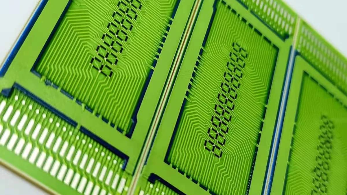
Overview
Multilayer routing in a fired ceramic thick film circuit is a stack-and-sequence decision, not a direct copy of plated-through FR4 practice. This page owns the net, stack, and routing-release review; general crossover explanation and the print-fire manufacturing sequence remain separate canonical topics. this guide maps net crossings, printed dielectric windows, conductor crossovers or metallized transitions, registration, refire history, and inspection access without treating a proposed construction as an approved manufacturing capability or a published dimensional rule set.
Engineering review matrix
Each row links a design variable to evidence that can support a drawing or release decision.
| Variable | Control question | Verification route |
|---|---|---|
| Construction boundary | Identify fired ceramic thick film, printed crossover, or metallized transition explicitly; do not use multilayer as an umbrella for LTCC, HTCC, thin film, or FR4 via structures. | Match the route name to the drawing stack, material records, and actual process sequence. |
| Layer and refire sequence | Record print, dry, fire, inspection, and protection order for every functional layer, including any repeated thermal exposure. | Review the complete traveller or proposed sequence and correlate it with representative processed samples. |
| Conductor-dielectric compatibility | Treat adhesion, wetting, shrinkage, topography, chemical interaction, and later assembly exposure as properties of the named material stack. | Use current supplier data and construction-specific trials; do not transfer a result from a different stack. |
| Registration budget | Allocate artwork, screen, substrate, firing movement, and inspection datum contributions around the smallest functional overlap or isolation feature. | Measure registered features on representative processed parts using the released datum scheme. |
| Crossover or via geometry | Define landing areas, neck-downs, dielectric windows, conductor overlap, topographic steps, and keep-outs around each vertical or crossing transition. | Inspect continuity and isolation at the transition; add sectional evidence only when an approved method and sample plan exist. |
| Electrical and thermal duty | Assign voltage difference, current, pulse, duty, resistance contribution, heat path, and permitted temperature rise to the actual routed feature. | Test the representative route at stated boundary conditions without converting a coupon result into a universal rating. |
| Assembly interface | Reserve pad, bond, solder, adhesive, component, coating, and mechanical keep-outs before the routing stack is frozen. | Review the downstream assembly drawing and inspect access after the final printed layer. |
| Probe and inspection access | Provide observable intermediate states or test points for faults that would be hidden after later printing or assembly. | Demonstrate that the released inspection and electrical methods can isolate an open, short, or insulation defect. |
Stack and routing release method
The order makes assumptions and ownership visible before a result is promoted to a requirement.
- 01
Name the construction family
State whether the design is sequentially printed and fired on a ceramic surface. Keep LTCC, HTCC, thin-film deposition, plated-through FR4, and other internally routed constructions outside this page unless they receive their own review.
- 02
Map nets before adding layers
Classify signal, supply, return, sense, and guarded nodes; record potential differences, current paths, thermal coupling, assembly interfaces, and the crossings that cannot be removed by placement or first-layer rerouting.
- 03
Build the printed sequence
Define each conductor, dielectric, crossover, and metallized transition in process order. Set lands, overlaps, registration allowances, edge boundaries, and inspection access from reviewed material and process evidence rather than generic layout values.
- 04
Prototype the critical transitions
A project validation plan may use representative coupons or prototype artwork to examine continuity, isolation, registration, dielectric coverage, topography, and refire interaction under the agreed electrical and environmental conditions.
- 05
Release a layer-controlled package
Issue layer artwork, sequence, material identifiers, datums, inspection stages, test limits, exception handling, and revision links as one controlled package. Any stack or material change reopens the affected checks.
- 06
Review fault containment and inspectability
For every transition, identify the credible open, short, leakage, registration, topography, refire, and assembly-interference faults, then decide at which printed state each fault can still be observed. Allocate intermediate visual or electrical checks before a later dielectric, conductor, protection layer, or component hides the feature. The review should connect each check to a net, datum, method, acceptance rule, sample stage, and disposition owner rather than relying on one final continuity test that cannot locate or explain a buried defect.
Failure controls
These are review prompts, not evidence that every risk applies or that every test is available.
- A
A printed crossover described as an internal multilayer structure, creating the wrong supplier and inspection assumptions
- B
Registration loss reducing conductor overlap or dielectric isolation at a transition
- C
Pinholes, edge thinning, or topographic voids leaving an unintended leakage or shorting path
- D
Conductor neck-down or current crowding producing local heating at a landing or crossover
- E
Repeated firing changing an earlier conductor, resistor, dielectric, or interface outside its reviewed state
- F
A buried defect becoming untestable after the next print or assembly operation
- G
Layer artwork, material revision, and traveller revision drifting out of alignment
Reference boundary
Public method sources
These sources support the engineering method and terminology used in this technical guide. They do not establish a ThickFilmPCB material list, capability limit, customer result, certification, or finished-product specification.
- 01NASA CR-120619 — Thick-film multilayer ceramic circuitry design guidelines
Supports the historical engineering model of sequential conductor and dielectric build-up, interlayer connections, fabrication, assembly, and reliability review only; it supplies no current ChipSimple design rule or modern dimensional limit.
- 02DuPont LF181 silver via-fill conductor technical data sheet
Supports reviewing via-fill level, capture-pad geometry, dielectric compatibility, refire exposure, encapsulation, and process sequence as linked decisions for one named material system; no dimensional or electrical value is transferable to ChipSimple production.
- 03DuPont 6444 multilayer dielectric technical data sheet
Supports coupling printed dielectric thickness, resolution, layer count, conductor compatibility, substrate, and firing for one named material system only; its laboratory values do not establish a general routing limit or ChipSimple performance.
Inputs for a practical review
Unknown values may be labelled unknown. The review should convert uncertainty into an explicit decision or validation task.
Send Drawings- 01
Complete netlist or schematic with signal, supply, return, sense, and guarded nodes identified
- 02
Layer-by-layer artwork, finished outline, datums, and required conductor crossings
- 03
Proposed substrate, conductor, dielectric, resistor, and protection material families
- 04
Working, transient, fault, current, pulse, duty, and thermal boundary conditions
- 05
Crossover, metallized transition, overlap, isolation, and keep-out requirements
- 06
Assembly interfaces including soldering, bonding, components, coatings, fixtures, and connectors
- 07
Continuity, resistance, insulation, dimensional, visual, and environmental acceptance methods
- 08
Prototype quantity, revision control, evidence deliverables, and change-approval responsibility