
Overview
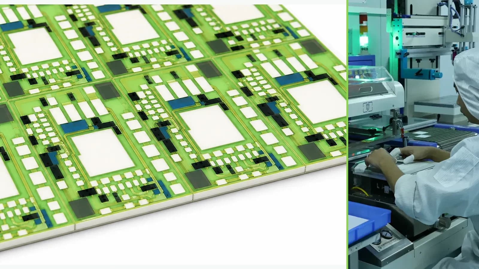
Silver-palladium conductor selection is a complete interface and process decision, not a choice based on metal names or a single resistivity value. The exact Ag/Pd ratio and glass or binder system, substrate, surface, screen, dried and fired thickness, line width, atmosphere, furnace profile, refires, resistor and dielectric compatibility, solder or wire-bond process, protection, electric field, contamination, humidity, fluids, and thermal-mechanical loads determine whether a named paste is relevant. Increasing palladium content is often discussed as a trade against cost, conductivity, migration, leaching, and interface behavior, but no direction or magnitude should be generalized without current data for the exact product and construction. A paste intended for a fuel-sensor application is not automatically suitable for a hybrid circuit, high-current feed, fine wire-bond pad, or another chemical environment. This guide shows how to screen supplier documentation and qualify a production-intent material stack. It does not claim that the photographed circuit uses Ag/Pd, that any supplier value is a ThickFilmPCB capability, or that one conductor family has been approved for a drawing.
Engineering review matrix
Each row links a design variable to evidence that can support a drawing or release decision.
| Variable | Control question | Verification route |
|---|---|---|
| Ag/Pd paste identity | Record manufacturer, product code, alloy or composition description exactly as documented, lot, shelf state, storage, conditioning, mixing, thinner, and substitution rule. | Use current TDS and receiving records; do not infer chemistry from color, trade name, or photographed appearance. |
| Substrate and material stack | Define ceramic grade and surface, conductor, resistor, dielectric, protection, pad finish, joint material, layer order, overlaps, and compatible families. | Qualify the complete processed stack and inspect interfaces after every relevant refire and assembly exposure. |
| Print and fired geometry | Specify screen, emulsion, artwork, wet and fired width, thickness, line edge, turns, necks, overlaps, pads, spacing, and registration. | Measure production-intent features and correlate geometry with resistance, current distribution, adhesion, and interface results. |
| Firing and refire history | Record drying, atmosphere, furnace load, profile, peak, time, cooling, number and order of refires, and later thermal operations. | Retain traceable profile and witness data after each critical exposure; do not treat a setpoint as a complete process record. |
| Electrical loading | Define current, voltage, pulse, duty, frequency where relevant, acceptable drop and heating, ground and bias conditions, and fault current. | Measure voltage, current, resistance, and temperature on production-intent geometry through nominal, tolerance, transient, and fault states. |
| Solder or wire-bond interface | Specify joint route, metallurgy, flux, solder, wire, tool, process parameters, dwell, pad geometry, cleaning, rework, strain relief, and test method. | Inspect and test actual joints before and after thermal, mechanical, and environmental conditioning; classify failure location. |
| Migration and corrosion environment | State humidity, condensation, fluid, sulfur or other contaminants, ionic cleanliness, electric field, spacing, protection, bias duration, and temperature. | Use biased and unbiased controls, defined inspection, insulation or resistance measurements, microscopy, and agreed acceptance criteria. |
| Change and evidence control | List paste, raw material revision, substrate, screen, profile, refire, protection, joint, cleaning, environment, or supplier changes requiring review. | Maintain drawing- and lot-linked travelers, source documents, coupon results, reviewer decisions, and requalification records. |
Controlled model
Conductor resistance, loading, and interface model
Translate a supplier sheet-resistivity value into a first geometry estimate only after matching fired thickness and test conditions. Then add terminations, corners, vias if present, solder or bond pads, local heating, electric field, environmental exposure, and process interactions.
R_line ≈ R□ × L/W = ρL/(Wt)First-order resistance of a uniform rectangular fired conductor expressed by sheet resistance or bulk resistivity.
- Units
- R in Ω; R□ in Ω/□; ρ in Ω·m; L, W, t in consistent length units
- Use boundary
- Assumes uniform thickness and current distribution. Printed edges, pores, necks, turns, overlaps, interfaces, refires, and supplier test geometry require coupon correlation.
V_drop = IR_line; P_line = I²R_lineElectrical drop and heat generated in the conductor for a stated current.
- Units
- V_drop in V; P in W; I in A; R in Ω
- Use boundary
- Does not establish current capacity or temperature. Pulse, duty, ambient, substrate and interface heat paths, terminals, neighboring layers, and fault current must be modeled and tested.
J_nom = I/(Wt)Nominal current density in a uniform rectangular cross-section.
- Units
- A/m² or A/mm²
- Use boundary
- Printed thickness and width are nonuniform, and current crowds at turns, necks, holes, contacts, and conductor transitions. Use local geometry and measured dimensions.
ΔR/R₀ = (R_after − R₀)/R₀Normalizes conductor-path change after firing, refiring, joining, thermal cycling, humidity, chemicals, or load.
- Units
- Dimensionless, commonly % or ppm
- Use boundary
- State temperature, current, contact method, elapsed time, conditioning, recovery, and measurement uncertainty. Resistance change alone does not identify migration, corrosion, cracking, or interface damage.
Decision comparison
| Decision | Route A | Route B | Verification |
|---|---|---|---|
| Higher-silver versus higher-palladium composition | A specific higher-silver product may offer a different resistance, cost, firing, leach, migration, corrosion, and joining balance under its supplier test conditions. | A specific higher-palladium product may shift those same tradeoffs, but metal ratio alone cannot predict the finished film because glass, additives, thickness, substrate, and process also matter. | Compare current TDS data only within stated methods, then print both candidates in the same production-intent geometry and stack and run the real electrical, interface, and environmental tests. |
| Solderable versus wire-bond interface | Soldering introduces alloy, flux, wetting, leaching, dwell, reflow cycles, cleaning, pad geometry, joint strain, and post-assembly inspection. | Wire bonding introduces wire and pad metallurgy, surface state, thickness, bond tool, force, ultrasonic or thermal parameters, loop, pull or shear method, contamination, and substrate support. | Select a paste whose supplier scope includes the intended interface, then qualify the complete production joint; one interface result does not approve the other. |
| Bare versus protected conductor | An exposed path or contact leaves the fired surface available but directly encounters moisture, contamination, abrasion, fuel or other media, and electric-field stress. | An overglaze, overcoat, seal, or housing can reduce some exposure while adding coverage edges, pinholes, trapped contamination, compatibility, stress, repair, and inspection boundaries. | Test the actual protection architecture and intentional openings through the selected environment and electrical bias. |
- A supplier firing peak is a processing condition for that named paste and test stack; it is never a finished circuit operating-temperature rating.
- Migration, corrosion, and leaching are different mechanisms and require their own environment, bias, joint, inspection, and acceptance definitions.
Failure controls
These are review prompts, not evidence that every risk applies or that every test is available.
- A
Selecting by nominal Ag/Pd ratio or metal name while glass system, substrate, thickness, geometry, firing, and companion layers remain unmatched
- B
Transferring supplier typical resistance, adhesion, migration, leach, or bond data from its test construction into a company capability claim
- C
Optimizing low line resistance while local turns, necks, pads, overlaps, or terminals create current crowding, heating, or weak interfaces
- D
Calling a paste solderable or wire-bondable without qualifying the exact joint materials, process, cleaning, pad geometry, loads, and conditioning
- E
Confusing corrosion, electrochemical migration, and solder leaching or using one test as evidence for all three mechanisms
- F
Changing paste lot family, thinner, screen, furnace atmosphere, profile, refire count, protection, solder, or cleaning outside controlled review
Silver-palladium conductor selection workflow
The order makes assumptions and ownership visible before a result is promoted to a requirement.
- 01
Define conductor functions
Identify interconnect, termination, solder pad, wire-bond pad, contact, electrode, resistor termination, via fill if applicable, or another function. State current, voltage, pulse, duty, loss, environment, assembly, inspection, and failure consequences for each region.
- 02
Lock substrate and companion layers
Name substrate grade and finish, resistor, dielectric, overglaze or overcoat, terminal finish, solder, wire, adhesive, coating, and layer order. Confirm which interactions and refires the selected supplier documents actually cover.
- 03
Screen named supplier products
Review product code, Ag/Pd description, intended application, rheology, screen, thickness, drying, firing, atmosphere, refires, resistivity, adhesion, leach or bond scope, storage, compliance statements, test geometry, and disclaimers. Keep candidate evidence separate.
- 04
Design current and interface geometry
Set width, effective thickness, length, turns, necks, current crowding, overlaps, spacing, edge distance, pad size, attachment, protection openings, thermal path, and test witnesses. Include artwork and process tolerances rather than nominal shapes alone.
- 05
Build production-intent coupons
Use traceable substrate and paste lots, production screen, printing, leveling, drying, furnace atmosphere and profile, refires, resistor and dielectric sequence, protection, soldering or bonding, cleaning, rework, and storage. Retain control and diagnostic structures.
- 06
Validate electrical and interfaces
Measure fired geometry, thickness, line and contact resistance, adhesion and failure plane, solderability or bond response, leaching, thermal behavior, isolation and visual condition where relevant, with calibrated methods and declared uncertainty.
- 07
Validate environment and freeze
Apply temperature, humidity, condensation, bias, fluids, contaminants, corrosion, vibration, shock, current cycling, and life sequence as required. Release only the named stack and profile, with sampling, records, reviewers, and material or process change triggers.
Reference boundary
Public method sources
These sources support the engineering method and terminology used in this technical guide. They do not establish a ThickFilmPCB material list, capability limit, customer result, certification, or finished-product specification.
- 01Heraeus C2240 Silver/Palladium Conductor technical data sheet
Supports the named product's Ag/Pd description, intended sensor use, printing, drying, firing, thickness, resistance, adhesion, leach, storage, and stated laboratory boundaries only; it proves no ThickFilmPCB result.
- 02Heraeus C2130B Silver/Palladium Conductor technical data sheet
Supports reviewing metallization, fired thickness, solder system, leach resistance, adhesion, substrate, and processing together for one separate named paste; values and compatibility cannot be combined with another product.
- 03NASA TM-2011-216463 — Ceramic and PCB interconnect test vehicles
Provides a primary test-study example in which ceramic substrate, Ag/Pd metallization, pad geometry, attach route, thermal cycling, and vibration are defined together; its construction and results are not supplier or ThickFilmPCB capability data.
Inputs for a practical review
Unknown values may be labelled unknown. The review should convert uncertainty into an explicit decision or validation task.
Send Drawings- 01
Circuit drawing identifying conductor functions, current paths, voltage and bias, pulse and duty, allowable drop or heating, spacing, pads, terminals, and protection openings
- 02
Exact substrate grade and finish, resistor, dielectric, overglaze or overcoat, joint, adhesive, coating, and material compatibility constraints
- 03
Candidate or mandated Ag/Pd supplier product codes, composition and compliance documents, storage, shelf, lot, thinner, and allowed-substitution rules
- 04
Print, dry, firing atmosphere and profile, fired thickness, refires, trim, protection, soldering or wire bonding, cleaning, rework, and assembly history
- 05
Solder alloy and flux or bond wire and tool, pad geometry, process conditions, joint loads, strain relief, visual, pull, shear, leach, or wetting criteria
- 06
Temperature, humidity, condensation, fluids, sulfur or other contaminants, ionic cleanliness, bias, corrosion, vibration, shock, and cycling conditions
- 07
Prototype matrix, coupons, sampling, measurement uncertainty, environmental sequence, acceptance rules, report fields, traceability, reviewers, and change control