
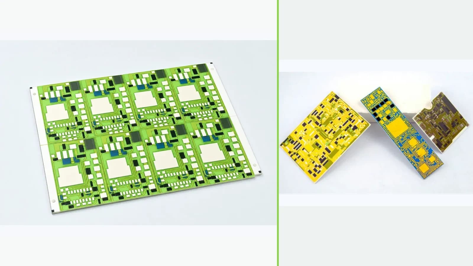
Overview
Conductive epoxy and solder are two distinct ways to create an electrical attachment on a thick-film circuit, but neither route is universally lower risk. Solder forms a metallic joint through alloy, flux, wetting and a controlled thermal profile; conductive epoxy forms a composite path through resin, conductive filler, bond-line geometry and cure. Each route changes electrical resistance, heat transfer, pad interaction, assembly temperature, cleaning, mechanical compliance, rework, storage, moisture behavior, corrosion risk and inspection. A comparison must begin with the exact fired pad, component or terminal finish, current and voltage, package geometry, environment and lifecycle rather than with generic statements about low temperature or high conductivity.
Engineering review matrix
Each row links a design variable to evidence that can support a drawing or release decision.
| Variable | Control question | Verification route |
|---|---|---|
| Fired pad and finish | Define conductor chemistry, fired thickness observation, pad geometry, finish material/thickness, surface preparation, protection opening, firing/refires, storage and handling. | Inspect and identify representative pads before joining, then correlate interface condition with electrical and failure-mode evidence. |
| Joining material | Name solder alloy and flux or conductive adhesive product and revision, material lot, storage, shelf/out time, preparation, supported surfaces, approved alternatives and restrictions. | Retain material genealogy and supplier instructions with every process record and test sample. |
| Joint geometry | Set overlap, volume, bond line or standoff, fillet or edge, void criteria where applicable, conductor entry, terminal alignment, joint count, access and tolerances. | Use drawing-linked visual, dimensional, section, imaging or other justified construction evidence appropriate to the route. |
| Electrical and thermal path | Define current waveform, voltage, allowable drop, power, neighboring heater/component heat, pad and terminal conduction, substrate, enclosure, ambient and fault states. | Use four-wire or justified electrical measurement plus local thermal mapping in the finished mounted assembly. |
| Mechanical load path | Allocate terminal/component mass, CTE mismatch, substrate support, lead compliance, strain relief, assembly tolerance, peel/shear/bending, vibration, shock and thermal cycles. | Apply representative loads with the real support and routing and record joint, pad, substrate and terminal failure modes. |
| Process and cleanliness | Define application, placement, profile or cure, atmosphere, fixture, cooling, cleaning, residue, handling, inspection holds, rework and downstream encapsulation/assembly. | Record actual temperature-time or cure evidence and inspect cleanliness and circuit changes after each controlled stage. |
| Environment and change control | Set temperature, humidity, condensation, fluids, corrosion, storage, powered state, cycling, acceptance drift, sampling, supplier/material/process changes and substitutions. | Test configuration-linked samples and reopen affected qualification whenever an interface, material, geometry, process or environment changes. |
Controlled model
Attachment-stack electrical, thermal, and mechanical comparison
Model the complete path from printed pad through finish and attachment to the component termination. Initial electrical resistance is only one outcome. Joint-area distribution, voids, filler network or alloy microstructure, interfaces, temperature, current crowding, compliance, cure or reflow history, residues and environment control the useful result. Product-level evidence must retain the named material lots and process history.
R_joint ≈ ρ_eff L_b/A_effFirst-pass joint resistance from effective resistivity, bond-line or joint length, and effective conductive area.
- Units
- R in Ω; ρ in Ω·m; L in m; A in m²
- Use boundary
- Effective properties are process- and temperature-dependent. Filler contacts, alloy phases, voids, interfaces, current crowding, oxidation, cure or reflow and aging require measurement.
P_joint = I²R_jointElectrical heat generated in the defined joint resistance at current.
- Units
- W
- Use boundary
- Does not predict temperature without neighboring component and heater heat, pad and lead conduction, substrate, enclosure, convection, transient duty and local current distribution.
ΔL_free = (α₁ − α₂)LΔTScreens differential free expansion between attached materials over a temperature change.
- Units
- Length
- Use boundary
- Not a joint stress or fatigue equation. Geometry, stiffness, joint thickness, viscoelasticity, plasticity, cure shrinkage, creep, gradients, constraint and cycling must be considered.
Decision comparison
| Decision | Route A | Route B | Verification |
|---|---|---|---|
| Pad and termination compatibility | Solder requires a compatible fired metallization or finish, component termination, alloy, flux, wetting behavior, resistance to metallization dissolution, profile, cleaning and post-joint surface state. | Conductive epoxy requires compatible pad and termination surfaces, resin/filler chemistry, controlled bond line, cure, adhesion, contact formation, storage and contamination control. | Use the exact pad-finish-termination stack and evaluate construction, initial electrical behavior, physical integrity and defined downstream/environmental effects. |
| Assembly thermal exposure | Solder applies a reflow, hot-bar, iron or other named heat cycle that can affect resistors, overglaze, substrate, components, previous joints and flux residues. | Epoxy uses a cure that may reduce peak temperature but adds time, pressure/fixturing, shrinkage, incomplete cure, moisture and later thermal-exposure questions. | Record the actual temperature-time history at representative locations and measure affected circuit and joint characteristics before and after assembly. |
| Mechanical accommodation | A metallic joint may be relatively stiff or ductile depending on alloy, geometry, thickness and temperature; fatigue and pad loading depend on the complete assembly. | An adhesive can be more compliant in some formulations, but modulus, glass transition, filler content, bond line, cure, creep and aging govern behavior. | Test representative joints in the production-intent geometry through the actual thermal and mechanical load spectrum and record failure mode. |
| Inspection and rework | Solder offers established visual and process criteria when the applicable standard and joint class are selected, while hidden interfaces and pad dissolution still need appropriate evidence. | Conductive epoxy appearance may not reveal cure, filler network, voids or interface adhesion, and removal/rework can damage the pad or leave residue. | Define route-specific inspection, electrical, construction, mechanical, environmental and rework validation rather than using one shared visual rule. |
- Electrical continuity after assembly cannot establish pad adhesion, joint integrity, cure, wetting, void condition, fatigue, corrosion, or long-term resistance stability. Record how and where a joint fails, not only whether its measured force or resistance crossed a limit.
- A low-temperature cure is not automatically gentler to the product: cure duration, shrinkage, fixture pressure, moisture, contamination, later soldering, operating temperature, creep and chemical exposure can dominate. Likewise, a solder profile is not acceptable merely because its peak is below a supplier maximum; the complete thick-film stack and component must be reviewed.
Failure controls
These are review prompts, not evidence that every risk applies or that every test is available.
- A
Choosing solder or conductive epoxy from a generic temperature or conductivity comparison without naming pad, termination, material, geometry, process and environment.
- B
Assuming solderability from a conductor label or adhesive compatibility from initial continuity without actual fired-pad and terminal evidence.
- C
Using identical joint geometry and inspection criteria for two attachment mechanisms whose material flow, bond line, fillet, void, cure and failure modes differ.
- D
Ignoring flux or adhesive residues, cleaning access, moisture, ionic contamination, corrosion, incomplete cure, solder dissolution, storage and rework effects.
- E
Transferring a lap-shear or coupon resistance result to a terminal or component with different stiffness, current entry, pad, peel load, heat path and cycling.
- F
Treating the photographed hybrid assemblies as evidence that either attachment route, material, process, strength, reliability or company capability is available or qualified.
Attachment-route comparison workflow
The order makes assumptions and ownership visible before a result is promoted to a requirement.
- 01
Define joint function and loads
State electrical current and voltage waveforms, allowable drop and heating, thermal path, component or terminal mass, alignment, clamp or peel load, vibration, shock, thermal cycling, humidity, fluids, contamination, storage, service, rework, and product-level acceptance.
- 02
Identify exact interface materials
Name fired thick-film pad, finish, substrate, protection opening, component or terminal base and plating, solder alloy/flux or epoxy resin/filler, cleaning agents, strain relief, encapsulant, and every downstream heat or chemical exposure. Do not compare unnamed families.
- 03
Design route-specific geometry
Set pad area, conductor entry, joint overlap, solder fillet or adhesive bond-line target, standoff, volume, gap, masks, edge clearances, neighboring heat-sensitive features, inspection access, terminal support, fixture, and tolerances for each route rather than sharing one drawing blindly.
- 04
Control process and handling
For solder, define preparation, alloy, flux, application, profile, atmosphere, dwell, cooling, cleaning and rework. For epoxy, define storage, thawing/conditioning, mixing if applicable, dispense, open time, placement, pressure, cure, post-cure and contamination. Record actual lots and histories.
- 05
Build comparable evidence
Use the same application boundary and relevant sample geometry, while applying route-appropriate inspection. Measure initial and powered resistance, local temperature, joint geometry, physical condition, pad interaction, mechanical response and residues; preserve failure locations and construction evidence.
- 06
Validate lifecycle and freeze selection
Run the specified thermal, humidity, chemical, vibration, mechanical, electrical-load, storage and rework sequence with intermediate checks. Approve only the exact pad, termination, joining material, geometry, process, cleaning, support, environment and acceptance method represented by the evidence.
Reference boundary
Public method sources
These sources support the engineering method and terminology used in this technical guide. They do not establish a ThickFilmPCB material list, capability limit, customer result, certification, or finished-product specification.
- 01IPC official overview of J-STD-001J and IPC-A-610J
Supports distinguishing soldering process/material requirements from post-assembly acceptance at a high level. Detailed criteria require applicable licensed standards; this overview does not qualify a thick-film joint.
- 02IPC J-STD-003D — Solderability tests for printed boards
Supports solderability and resistance-to-dissolution method boundaries within its scope only. It does not select a pad, joint alloy or application design.
- 03NASA-STD-8739.3 — Soldered Electrical Connections
Supports controlled soldered-connection workmanship, process and verification concepts within its scope. It is not evidence of ChipSimple soldering or a conductive-adhesive comparison result.
- 04NIST Technical Note 1297 — measurement uncertainty
Supports uncertainty treatment when comparing resistance, temperature, geometry and mechanical measurements; it provides no attachment performance value.
- 05NASA — Investigation of discrete-component chip mounting technology for hybrid microelectronic circuits
Provides a direct historical experiment comparing specified gold-filled conductive adhesives and solder alloys on defined thick- and thin-film ceramic metallizations before and after selected screening exposures. It does not establish that a modern adhesive or solder is universally superior, nor does it prove a ThickFilmPCB process or lifetime.
- 06IBM Research — Evaluation of contact resistance for isotropic electrically conductive adhesives
Provides direct study evidence that adhesive-joint contact resistance and stability depend on the specific adhesive and copper-surface metallization under the tested stresses. The study does not make all conductive adhesives solder-equivalent or establish complete assembly thermomechanical life.
- 07Electrical reliability of conductive-adhesive joints — curing and current-density study
Provides direct experimental evidence that curing condition and current density affected the electrical behavior and degradation of the tested silver-filled epoxy joints. Its material, cure, geometry, loading, and life results cannot be transferred to another adhesive or production process.
Inputs for a practical review
Unknown values may be labelled unknown. The review should convert uncertainty into an explicit decision or validation task.
Send Drawings- 01
Fired pad and protection drawing, conductor/finish requirements, substrate, firing/refires, surface preparation, storage, and approved material restrictions.
- 02
Component or terminal material, plating, mass, geometry, alignment, external leads, strain relief, mounting, connector and assembly load path.
- 03
Current and voltage waveform, allowable joint drop and temperature, duty, transients, neighboring heat, thermal interfaces, ambient and fault states.
- 04
Candidate solder/alloy/flux or conductive adhesive product, storage, application, profile/cure, atmosphere, fixture, cleaning, rework and downstream process.
- 05
Joint overlap, solder volume/fillet or adhesive bond line, standoff, void/construction criteria, tolerances, inspection access and sampling.
- 06
Thermal cycling, humidity, fluids, corrosion, vibration, shock, mechanical loading, powered exposure, storage, life-related and failure-mode criteria.
- 07
Prototype alternatives, sample quantities, process records, four-wire/thermal/construction/mechanical methods, reports, traceability, revisions and change triggers.