
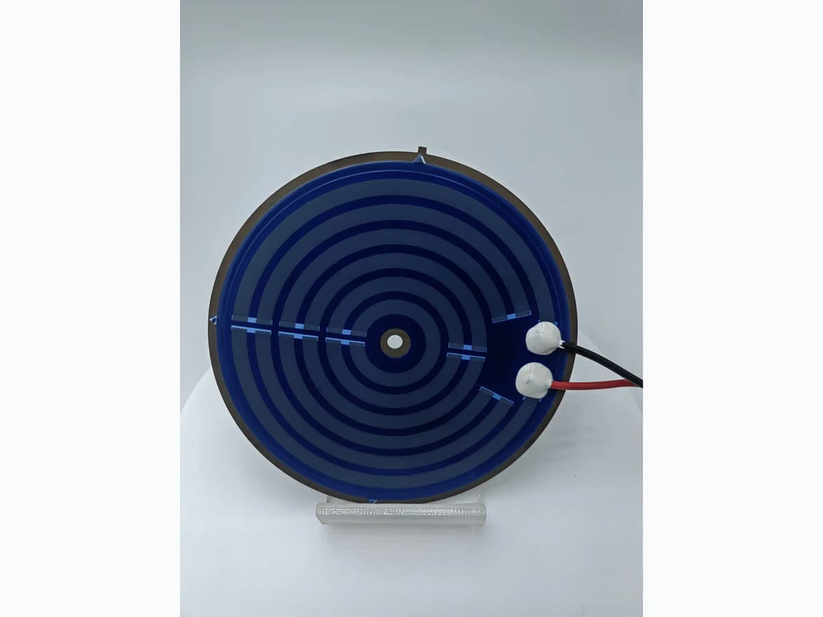
Overview
A heater terminal is an electro-thermal and mechanical transition, not merely a place to attach a wire. Current moves from a printed resistor through a conductor overlap, fired pad, optional finish, joint, terminal or lead, connector, and external harness while heat and mechanical strain follow different paths. The transition can fail through excessive voltage drop, local heating, pad damage, joint fatigue, conductor leaching, corrosion, insulation loss, or load transfer into brittle ceramic. A credible design defines every interface, attachment process, assembly heat exposure, support feature, accessible-metal boundary, and validation condition before choosing pad size or joining route.
Failure controls
These are review prompts, not evidence that every risk applies or that every test is available.
- A
Sizing a terminal only from average current while ignoring startup, controller pulses, temperature-dependent resistance, connector loss, and abnormal states.
- B
Using a solderable or bondable material label without verifying the exact fired pad, finish, heat history, joining chemistry, and post-process condition.
- C
Allowing a stiff lead, heavy tab, short routing span, or connector force to peel metallization or bend and crack a ceramic substrate.
- D
Measuring low initial resistance but missing localized joint heating, current crowding, voids, contamination, corrosion, or degradation after cycling.
- E
Placing terminals so close to active heater traces that joining heat, heat sinking, protection openings, or mechanical support disrupts the designed thermal field.
- F
Changing alloy, adhesive, plating, lead material, cleaning, cure, rework, or strain relief while assuming previous qualification automatically transfers.
Engineering review matrix
Each row links a design variable to evidence that can support a drawing or release decision.
| Variable | Control question | Verification route |
|---|---|---|
| Current and voltage path | Define RMS, peak, startup, fault and pulse current; working voltage; polarity; controller behavior; conductor widths; overlaps; joint interfaces; and connector contact path. | Use four-wire or otherwise justified measurements and synchronized waveform capture at defined temperatures to separate the terminal path from the heater body. |
| Pad and metallization system | Name pad material, fired thickness observation, geometry, surface condition, finish, refire history, conductor compatibility, edge distance, and protection opening. | Inspect representative fired pads and attachment cross-sections or surfaces as appropriate and retain material/process identity with the results. |
| Joining process | Specify solder, braze-like alloy, weld, conductive adhesive, mechanical contact, or other route with material, amount, temperature or cure, pressure, atmosphere, cleaning, and rework constraints. | Record the actual profile and process inputs, inspect joint formation and residues, and correlate initial and post-exposure electrical and mechanical evidence. |
| Local thermal field | Include heater-zone heat, joint I-squared-R loss, lead conduction, pad spreading, substrate, housing, convection, insulation, and fault or loss-of-load conditions. | Map temperature at fixed locations through warm-up and steady or cyclic duty in the real mounting, with sensor uncertainty documented. |
| Lead and strain relief | Set conductor gauge, stiffness, length, bend radius, orientation, support distance, anchor material, routing tolerance, connector loads, and assembly handling limits. | Apply representative routing, insertion, pull, bend, vibration, and thermal motion while monitoring the pad and substrate for damage and electrical change. |
| Insulation and accessible metal | Define dielectric coverage, creepage path, clearances, lead insulation, grounding, housing, contamination, humidity, working/transient voltage, and application safety boundary. | Review the complete assembled section and execute the project-selected leakage, insulation, and withstand methods under stated conditions. |
| Environment and change control | Identify temperature cycling, humidity, fluid or cleaning exposure, corrosion risk, vibration, storage, service, approved materials, suppliers, process revisions, and substitutions. | Use configuration-linked samples and repeat defined tests after changes that can alter the electrical, thermal, chemical, or mechanical interface. |
Controlled model
Terminal voltage-drop, heating, and load-path model
Treat the connection as a series of named electrical resistances and parallel thermal and mechanical paths. A milliohm-scale value may matter at heater current, but a low initial resistance does not prove joint stability. The model must retain contact area, current distribution, pad geometry, material compatibility, heat flow, support distance, lead motion, assembly sequence, and the application's insulation boundary.
V_drop = I R_pathRelates heater current to voltage lost across the complete terminal path.
- Units
- V_drop in V; I in A; R_path in Ω
- Use boundary
- R_path includes printed conductor, overlap, pad, finish, joint, terminal, lead, and contacts at the relevant temperature. Probe and lead resistance must be separated by the measurement method.
P_joint = I² R_jointScreens local electrical heating associated with a defined joint resistance.
- Units
- P_joint in W; I in A; R_joint in Ω
- Use boundary
- Does not predict joint temperature without local thermal paths, current crowding, neighboring heater heat, convection, and transient duty.
σ_nom = F / A_supportA simple nominal stress screen for load transmitted through an attachment or support area.
- Units
- σ in Pa; F in N; A in m²
- Use boundary
- Not a fracture or fatigue prediction. Peel, bending, wire stiffness, vibration, ceramic flaws, pad edge stress, joint geometry, temperature, and cyclic loading require representative analysis or test.
Decision comparison
| Decision | Route A | Route B | Verification |
|---|---|---|---|
| Soldered or brazed-style thermal attachment versus conductive adhesive | A metallic joint can offer a direct electrical path but requires a compatible pad system, controlled heat profile, wetting or alloy behavior, residue control, and strain management. | A conductive adhesive route uses a cured composite joint whose electrical, thermal, mechanical, cure, thickness, and environmental behavior must match the application. | Qualify the complete named pad-and-joint stack with four-wire resistance, thermal mapping, joint inspection, mechanical loading, and environment/cycling appropriate to the assembly. |
| Rigid terminal versus flexible lead transition | A rigid tab can simplify external connection but may transfer assembly tolerance, vibration, bending, and thermal expansion directly into the pad or substrate. | A compliant lead or shaped strain-relief loop can reduce transmitted load but adds resistance, motion, clearance, joining, and handling variables. | Measure displacement and load at the ceramic interface and inspect electrical and physical condition before and after representative routing, assembly, vibration, and thermal cycling. |
| Large pad versus controlled current entry | A larger pad provides attachment and inspection area, yet it also changes heat spreading, thermal mass, material consumption, and distance from the active resistor. | A compact pad saves area but can concentrate current or mechanical stress and leave inadequate process, probe, or insulation margin. | Use current-path analysis and product-level temperature, resistance, pull or shear where applicable, and section/visual evidence against drawing-defined acceptance criteria. |
- Terminal pull or shear testing belongs to a defined quality method with specimen, loading direction, rate, fixture, failure mode, and acceptance criteria; this design page does not claim such equipment or results.
- Flux, cleaning chemistry, adhesive cure, rework, and downstream assembly heat can affect the printed stack and must be part of the material compatibility review.
Terminal-interface design sequence
The order makes assumptions and ownership visible before a result is promoted to a requirement.
- 01
Define external and internal loads
Document voltage, current waveform, startup and fault states, conductor temperature, ambient, heated-zone proximity, lead or terminal mass, connector insertion, wire routing, handling, vibration, shock, thermal cycles, and any service movement. State which loads act during manufacturing, installation, normal use, and abnormal use.
- 02
Specify the complete material stack
Name substrate, resistor, conductor overlap, fired pad material, optional finish, joining alloy or adhesive, terminal metal and plating, lead insulation, protective layers, flux or cleaning chemistry, and downstream processes. Compatibility must be reviewed as a complete system rather than inferred from one material name.
- 03
Shape the current and heat transition
Dimension the resistor-to-conductor transition, pad entry, attachment area, conductor width, current-spreading features, separation from active heat, and local heat sinks. Review nominal and tolerance resistance, contact area, temperature dependence, and the possibility of hidden local heating beneath a joint.
- 04
Create a mechanical load path
Place strain relief, compliant lead features, adhesive support if applicable, routing anchors, housing supports, and assembly fixtures so normal handling and service loads do not peel the pad or bend the brittle substrate. Keep support methods from violating insulation or trapping harmful residue.
- 05
Plan joining and inspection
Define pad preparation, deposition or attachment amount, temperature and time profile, pressure, cure, atmosphere, cleanliness, rework limits, visual criteria, dimensional checks, electrical measurement, and failure-mode recording. Use drawing references and configuration traceability for every inspected sample.
- 06
Validate the finished connection
Test the production-intent heater with real lead routing and mounting under electrical load, thermal duty, assembly handling, mechanical exposure, and relevant environment. Compare voltage drop, local temperature, insulation behavior, joint and pad condition, and resistance change before and after the matrix.
Reference boundary
Public method sources
These sources support the engineering method and terminology used in this technical guide. They do not establish a ThickFilmPCB material list, capability limit, customer result, certification, or finished-product specification.
- 01NASA-STD-8739.4 — Crimping, Interconnecting Cables, Harnesses, and Wiring
Supports disciplined definition, workmanship, inspection, routing, support, and documentation for wiring and interconnects within its stated scope. It does not prescribe a thick-film pad stack or prove ChipSimple harness or heater-terminal capability.
- 02IPC official overview of J-STD-001J and IPC-A-610J
Supports distinguishing soldering process/material requirements from post-assembly acceptance at a high level. Detailed contractual criteria require the applicable licensed standards; the overview does not qualify a ceramic heater joint.
- 03Heraeus — C2130B silver/palladium conductor technical data sheet
Supports reviewing one named fired conductor together with processing, fired thickness, adhesion, solder system, and leach-resistance test context only. Its values are not transferable to another pad, joint, assembly, or ChipSimple capability.
- 04IPC J-STD-003D — Solderability tests for printed boards
Supports terminology and test-method boundaries for solderability and resistance to dissolution of metallization within the standard's scope. It does not determine terminal geometry or establish product-level reliability.
Inputs for a practical review
Unknown values may be labelled unknown. The review should convert uncertainty into an explicit decision or validation task.
Send Drawings- 01
Heater schematic, supply and controller, cold/hot resistance states, current waveform, duty, startup, overload, transients, and fault behavior.
- 02
Dimensioned resistor-to-conductor overlap, pad and protection geometry, layer stack, substrate outline, edge distances, terminal locations, and tolerances.
- 03
Requested conductor, pad, finish, terminal, lead, insulation, joining material, flux or adhesive, cleaning, cure, atmosphere, and rework restrictions.
- 04
External lead gauge, stiffness, routing, bend radius, connector, support distance, strain relief, installation sequence, and mechanical load cases.
- 05
Heated load, mounting, local temperature field, ambient, fluid or airflow, enclosure, accessible metal, grounding, and insulation requirements.
- 06
Joining profile and assembly heat exposures plus electrical, visual, dimensional, mechanical, leakage, withstand, environmental, and cycling criteria.
- 07
Prototype and qualification quantities, sample configurations, traceability, report format, drawing revision, approved substitutions, and change-control triggers.