
On this page
- Size Conductors from Current and Temperature Rise
- Use Smooth Transitions and Controlled Corners
- Design Pads for the Actual Joining Process
- Separate Electrical Land Size from Registration Land Size
- Control Surface Condition Through Assembly
- A Worked Engineering Review
- Design Review Checklist
- Questions Engineers Commonly Ask
- Related Engineering Resources
- Closing Note
Prepared by Chipsimple Engineering Team, Engineering and technical content review
Published online August 10, 2026 · Reviewed August 10, 2026
ENGINEERING ARTICLE 05 / VOLUME 1
Conductor Lines, Pads and Terminations on Ceramic Thick Film Circuits
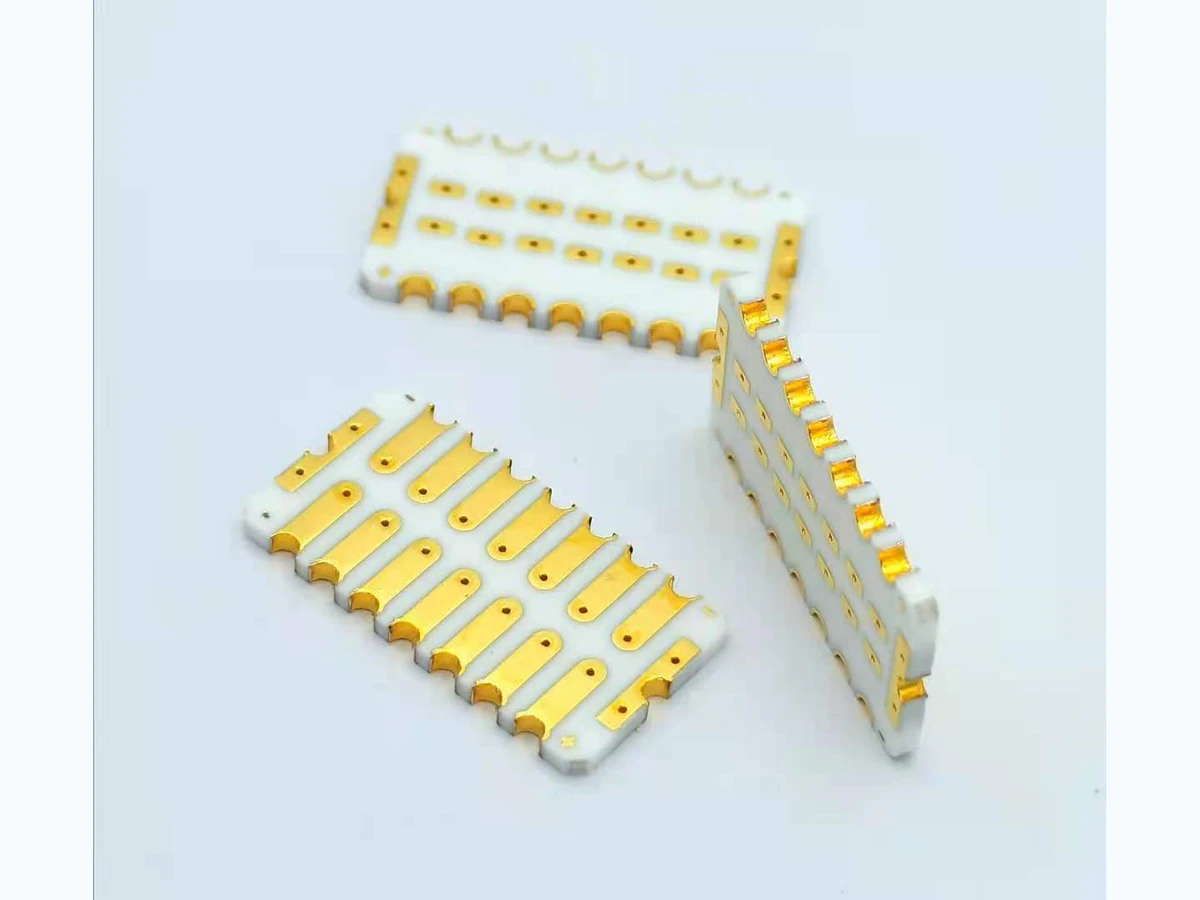
A thick-film conductor is a fired composite, not a miniature copper-clad trace. Its electrical and mechanical behaviour depends on paste chemistry, the substrate interface and the firing history. Pads may also face solder, aluminium or gold wire bonding, conductive adhesive, spring contact or brazed terminals. Each interface needs a compatible finish and a land pattern that controls stress.

Size Conductors from Current and Temperature Rise
A useful way to frame the decision is this: Allowable current cannot be assigned from width without fired thickness, resistivity, cooling and duty cycle. As a result, a short pulse path and a continuous current path with the same geometry may have very different limits. That cause-and-effect chain should remain visible when thick film conductor design is reviewed with purchasing and quality teams.
The manufacturing boundary is protected when the team can define RMS and peak current, pulse duration, repetition, ambient temperature and permitted rise. This approach separates the customer's functional need from the supplier's machine-specific compensation.
Confirm the decision with four-wire path resistance and powered thermal mapping on the actual ceramic assembly. Include both typical and boundary-condition specimens where the failure consequence justifies them.
The symptom a narrow neck or via land heating while the average trace width appears adequate deserves a structured investigation. Check material lot, artwork position, thermal history and measurement setup before assigning a single cause.
Use Smooth Transitions and Controlled Corners
Geometry and material meet at this point: Abrupt width changes concentrate current and printing variation. Therefore, inside corners, acute angles and small neck-downs can create local resistance, paste thinning and field stress. A nominal specification that omits the interface is incomplete even if every individual value looks reasonable.
During release, taper current transitions, avoid unnecessary acute corners and protect minimum neck width. Make sure the acceptance method measures the same physical feature that the design calculation assumed.
Useful confirmation includes magnified fired-pattern inspection and resistance comparison across representative geometries. Keep photographs or sections tied to part, revision, lot and orientation so they remain evidence rather than decoration.
One failure signature is repeatable hot spots or opens at the same artwork transition. It often becomes clear only when results are sorted by position, process stage or exposure instead of being combined into one average.
Design Pads for the Actual Joining Process
Process capability follows from the mechanism: Solder, wire bonding and conductive adhesive load pads differently. The direct implication is that solder can dissolve or embrittle some metallisations, wire bonding needs a clean compatible surface, and rigid terminals can peel the film. This makes the topic a design input, not merely a factory setting adjusted after the drawing is complete.
A practical release action is to identify alloy, flux, temperature-time profile, wire material or adhesive cure for every pad family. The requirement should survive staff changes and future lot reviews because it is recorded with the controlled construction.
Use joint pull, shear or adhesion testing after the intended thermal exposure to demonstrate margin. When feasible, compare the result before and after the operation most likely to disturb it.
Pay attention to good visual wetting or bond appearance followed by low mechanical strength or ageing drift. A corrective action is credible only when it changes that physical mechanism and the follow-up data confirm the change.
Separate Electrical Land Size from Registration Land Size
A via, crossover or component pad may need extra capture beyond its electrical contact area. The consequence is that registration error can reduce overlap even when the nominal artwork is centred. In a thick film conductor design review, this relationship deserves an explicit decision rather than an assumption copied from a previous drawing.
The practical control is to define the minimum remaining overlap at worst-case layer displacement. That instruction should be linked to the layer, material system or feature it governs so that production and inspection read it in the same way.
Verification should include first-article overlay measurements and cross-section review for critical buried interfaces. If the evidence is collected only after final assembly, the team loses the ability to separate printing, firing, trimming and assembly effects.
A common warning sign is partial capture that passes continuity but develops high resistance or cracks after cycling. Treat that symptom as a request to examine the process chain, not simply as a reason to widen the final tolerance.
Control Surface Condition Through Assembly
Storage, handling and repeated heat exposure can change the termination surface. The consequence is practical: fingerprints, oxidation, fired residue and excessive reflow time reduce bondability and solderability. This is one reason thick film conductor design cannot be reduced to a single catalogue value.
During design review, set packaging, shelf-life, cleaning and maximum thermal-exposure requirements for exposed pads. The objective is not to freeze every process setting on the customer drawing, but to define the functional boundary that the manufacturer must protect.
A useful evidence package contains incoming surface inspection and joining trials after representative storage or ageing. Comparing those records with the approved construction is more informative than judging an isolated photograph or one resistance reading.
Watch for lot-to-lot assembly yield variation with no change in artwork. It often indicates that two individually acceptable variables have combined at the edge of their windows.
A Worked Engineering Review
A ceramic power module may use a broad silver-based path for current, a different compatible surface on wire-bond pads and a low-current sense route near the same component. The layout review checks the smallest width after printing, the fired path resistance and the temperature at the narrow transition into the component land. It then checks whether the joining cycle attacks the conductor and whether the terminal stiffness loads the pad edge. If a plated or overprinted pad finish is proposed, the overlap and firing sequence become controlled interfaces. A coupon using the production pad stack is more useful than a generic adhesion value.
Design Review Checklist
- State peak, RMS and continuous current with duty cycle.
- Protect minimum necks and taper high-current transitions.
- Call out joining material and thermal profile per pad family.
- Define minimum overlap for vias, crossovers and overprints.
- Agree adhesion, pull, shear or solderability evidence.
Questions Engineers Commonly Ask
Can a current rating be given in amperes per millimetre of width?
Only as a preliminary rule with stated fired thickness, material, temperature rise and cooling condition. Final qualification should use the actual layout and duty cycle.
Why do conductor pads sometimes need a different metallurgy?
The best bulk conductor for cost and current may not be the best surface for soldering or wire bonding. A compatible overprint or finish can create a specialised interface.
Is visual inspection enough for pads?
No. Appearance cannot prove adhesion, bond strength, solder leaching resistance or ageing stability. Use process-specific mechanical and electrical tests.
Related Engineering Resources
Closing Note
Conductor design should end with evidence from the intended joining process. When current path, pad stack and assembly are reviewed together, the drawing becomes both electrically clear and manufacturable.