
Overview
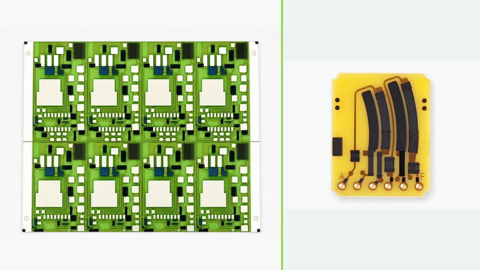
A fired thick-film resistor on ceramic and an embedded resistor inside a printed board can both remove a packaged component from part of a circuit, but they are different material, process, thermal, electrical, inspection, repair, and supply-chain systems. Ceramic thick film typically forms resistor material and conductors on a ceramic surface through a compatible print and firing sequence, with laser trim and protective layers available only when designed and qualified. PCB embedded resistors are incorporated within the organic printed-board construction using laminate-like resistive foil, plated or deposited systems, or printed nonlaminate materials under the applicable board design and performance specification. They experience imaging, etching or printing, lamination, drilling, plating, thermal excursions, moisture, and board assembly. Selection therefore begins with circuit function, impedance and parasitics, value and ratio, loading, thermal path, available area, layer architecture, trim or calibration strategy, test access, rework, board yield impact, qualification class, and supplier evidence. This page does not claim that ThickFilmPCB manufactures PCB embedded resistors, that the photographed external carbon track is embedded, or that either route is universally smaller, cheaper, more accurate, more stable, or more reliable.
Engineering review matrix
Each row links a design variable to evidence that can support a drawing or release decision.
| Variable | Control question | Verification route |
|---|---|---|
| Electrical function and value | Define resistance, ratio or transfer, nodes, tolerance, reference condition, TCR or tracking, voltage, power, pulse, noise, parasitics, and calibration. | Measure individual values and the loaded circuit response with route-specific fixtures and uncertainty. |
| Host material stack | Specify ceramic and fired layers or PCB laminate, resistive material, copper, dielectric, planes, vias, surface finish, protection, joints, and complete cross-section. | Review controlled drawings, material certificates where relevant, process travelers, sections, and visible construction evidence. |
| Resistor geometry and process | Set sheet-resistance family, effective L/W, thickness, corners, ends, overlaps, foil or print patterning, firing or cure, lamination, trim, and tolerance allowance. | Measure process witnesses and correlate actual geometry, thickness, value distribution, and failure features. |
| Thermal boundary | Define substrate or laminate heat paths, copper spreading, planes, vias, attachments, housing, interface, airflow, ambient, neighboring heat, gradients, duty, and faults. | Model and map production assemblies under representative loading and tolerance conditions. |
| Inspection and test access | Define in-process and final nodes, coupons, cross-sections, visual or imaging method, value test, isolation, thermal map, sampling, destructive evidence, and acceptance timing. | Demonstrate defect detection and measurement capability before features become inaccessible. |
| Trim, calibration, and repair | Specify physical trim or no-trim, calibration points and ownership, access, protection timing, retest, rework, board or module impact, scrap, and traceability. | Validate the full adjustment and disposition path without using software to hide unstable physical construction. |
| Environment and qualification | State operating and storage temperature, humidity, condensation, bias, fluids, vibration, shock, cycling, assembly, applicable IPC or other standard, class, addendum, and deviations. | Condition production-intent builds and compare electrical, thermal, mechanical, visual, sectioned, and failure baselines. |
| Supply and change control | Identify process owners, material revisions, supplier continuity, minimum lots, board and ceramic revisions, qualification scope, records, and requalification triggers. | Maintain approved bills, drawings, evidence packets, change notices, review decisions, and route-specific release records. |
Controlled model
Same-boundary resistor-route comparison
Compare both routes at the same nominal value, tolerance definition, reference temperature, voltage, power and pulse, circuit loading, area, thermal interfaces, environmental sequence, test access, calibration, production volume, and acceptance method. Keep supplier capability and process ownership explicit.
R ≈ R□(L/W) + R_end + R_interconnectFirst-order resistance model using sheet resistance, number of squares, end effects, and route-specific interconnect contributions.
- Units
- All resistance terms in Ω; R□ in Ω/□
- Use boundary
- The applicable sheet-resistance thickness convention, pattern process, corners, conductor overlaps, foil etch, lamination, firing, trim, contacts, and temperature require route-specific correlation.
P = I²R = V²/R; q'' = P/A_RElectrical dissipation and nominal resistor-area loading under a stated circuit condition.
- Units
- P in W; q'' in W/mm² or W/m²; V in V; I in A; R in Ω; A_R in mm² or m²
- Use boundary
- Does not set allowable power or temperature. Ceramic, copper, dielectric, laminate, planes, vias, package, airflow, pulse, duty, and fault paths differ between routes.
ΔR/R₀ ≈ αΔT + e_process + e_load + e_environment + e_timeA bookkeeping model for temperature, process, electrical load, environmental, and time-dependent fractional change.
- Units
- Dimensionless, commonly % or ppm; α in 1/K; ΔT in K
- Use boundary
- Terms may be nonlinear, correlated, history-dependent, and material-specific. Do not add them numerically without evidence and a declared combination method.
Y_system = Y_resistor-route × Y_host-process × Y_test-detectionConceptual reminder that integration yield depends on resistor and host manufacturing plus detection strategy.
- Units
- Dimensionless when factors are probabilities
- Use boundary
- Not a prediction or company metric. Dependencies and rework must be modeled from real process data; no yield value is supplied.
Decision comparison
| Decision | Route A | Route B | Verification |
|---|---|---|---|
| Host construction | Fired thick-film ceramic integrates resistor and conductor features on a ceramic substrate with a supplier-compatible firing, trim, protection, terminal, and module assembly route. | PCB embedded resistance becomes part of an organic board layer stack and must survive the defined imaging or printing, lamination, drilling, plating, board finish, assembly, and qualification sequence. | Review each complete cross-section, material list, traveler, ownership boundary, and qualification evidence; do not compare only the resistor film. |
| Thermal path and loading | A ceramic surface resistor couples heat through ceramic, printed layers, attachments, housing, interfaces, and ambient, with local trim and termination effects. | An embedded resistor couples into laminate, copper features, planes, vias, neighboring layers, resin, board surfaces, mounting, and airflow, with internal hot spots less directly visible. | Model and map production-intent assemblies under the same electrical duty and boundary, including internal or local temperature evidence appropriate to each route. |
| Trim, test, and repair | A surface ceramic resistor may permit laser trim and direct inspection before protection, depending on material, geometry, access, sequence, and qualified process. | An embedded element may require value targeting before or during board build, dedicated coupons and test access, and may be inaccessible after lamination; rework can affect the host board. | Define when every value is measured, how out-of-limit material is dispositioned, what can be calibrated, and which destructive sections or coupons verify hidden construction. |
| Integration objective | Ceramic thick film can combine resistors with ceramic thermal, dimensional, packaging, and hybrid-circuit functions in a distinct subassembly. | PCB embedding can reduce discrete placements or routing parasitics within the main board but increases material, design, documentation, fabrication, and test coupling to that board. | Use a system trade study including board or module area, interconnect, thermal, electrical, supply, qualification, cost model, yield evidence, and lifecycle—not a component-count slogan. |
- Embedded, buried, printed-on-board, and surface-printed resistors are not synonyms; use the actual construction and applicable specification terminology.
- The current IPC revision and selected performance class or addendum belong in procurement documents; an old table of contents is not a substitute for the licensed contractual standard.
Failure controls
These are review prompts, not evidence that every risk applies or that every test is available.
- A
Using embedded, buried, surface printed, and ceramic thick film as interchangeable terms and comparing the wrong constructions
- B
Comparing resistor films while ignoring host substrate, copper, dielectric, lamination or firing, joints, thermal boundary, assembly, and inspection
- C
Assuming PCB embedding automatically reduces cost or size without accounting for board yield, layer count, materials, coupons, test, scrap, and requalification
- D
Assuming ceramic thick film automatically gives precision or power capability without actual material, geometry, trim, thermal, measurement, and stability evidence
- E
Discovering value or hidden-layer defects after lamination or protection without planned test access, coupon correlation, disposition, and repair strategy
- F
Implying ThickFilmPCB manufactures or qualifies embedded PCB resistors, or using an external carbon-track photograph as embedded-construction proof
Resistor-route selection workflow
The order makes assumptions and ownership visible before a result is promoted to a requirement.
- 01
Define circuit and system need
Specify function, nodes, nominal values, ratios, source and load, voltage, current, power, pulse, frequency, parasitics, area, tolerance, temperature response, noise, stability, calibration, environment, safety, and failure behavior.
- 02
Draw complete route cross-sections
For ceramic thick film, include substrate, conductors, resistor, trim, protection, pads, joints, housing, and PCB connection. For embedded PCB, include resistive material, copper, dielectrics, layers, vias, lamination, surface finish, assembly, and board stack.
- 03
Map manufacturing ownership
Identify material suppliers, ceramic printer and firing owner, trim, protection, board fabricator, lamination, drilling, plating, assembler, calibration, inspection, laboratories, and acceptance authority. Do not imply ThickFilmPCB ownership of unverified embedded-board processes.
- 04
Model values and thermal loading
Use route-specific sheet-resistance, geometry, ends, interconnect, trim, voltage and power relations. Include tolerance distributions, temperature, gradients, pulse, planes, interfaces, contacts, assembly, and fault conditions without transferring material data.
- 05
Plan test access and disposition
Define when values are measured, accessible nodes, four-wire or other fixtures, coupons, cross-sections, thermal measurements, trim or calibration, retest, rework, scrap, hidden-defect detection, records, and board- or module-level escape risk.
- 06
Build comparable prototypes
Create production-intent builds of both viable routes with traceable materials and process histories. Test identical system requirements using route-appropriate inspection, assembly, environmental, electrical, thermal, mechanical, and measurement methods.
- 07
Select and control the route
Review evidence for performance, process variation, detection, repair, qualification, supplier continuity, cost model, volume, change control, and maintenance. Release one construction and reopen the trade after a material, host stack, duty, environment, or supply change.
Reference boundary
Public method sources
These sources support the engineering method and terminology used in this technical guide. They do not establish a ThickFilmPCB material list, capability limit, customer result, certification, or finished-product specification.
- 01IPC-6017A — Printed Boards Containing Embedded Devices
Supports the qualification and performance scope, documentation, process control, material, visual, registration, and test categories for printed boards containing embedded devices; detailed criteria require the licensed current standard and selected procurement requirements.
- 02IPC-2316 — Design Guide for Embedded Passive Device Printed Boards
Supports the distinction among discrete, array, integrated, and embedded passives and the need to integrate material, physical, thermal, design, and board-process considerations; it does not rank a ceramic route or prove capability.
- 03IPC-4811 — Embedded Passive Device Resistor Materials
Supports embedded resistor material categories, sheet-resistance geometry, conformance, characterization, and use with PCB design and performance standards; the revision table marks this document no longer maintained, so current contractual selection needs review.
- 04Heraeus R8900 Series thick-film resistor TDS
Supports the ceramic thick-film side as a named resistor material system whose properties depend on substrate, termination, geometry, print, firing, trim, and test conditions; supplier typical values are not ThickFilmPCB capabilities.
Inputs for a practical review
Unknown values may be labelled unknown. The review should convert uncertainty into an explicit decision or validation task.
Send Drawings- 01
Schematic and system requirements with resistor nodes, values, ratios, loading, voltage, power, pulse, frequency, parasitics, tolerance, TCR, noise, stability, and calibration
- 02
Candidate ceramic module and PCB embedded cross-sections with complete materials, dimensions, layers, conductors, resistor geometry, interfaces, joints, protection, and assembly
- 03
Host board or module constraints including area, thickness, layer count, thermal path, planes, vias, mounting, connectors, housing, airflow, ambient, and neighboring heat
- 04
Process ownership and supplier boundaries for materials, ceramic printing and firing, trim, PCB fabrication and lamination, plating, assembly, calibration, laboratories, and release
- 05
Applicable standards, performance class, addenda, procurement notes, inspection, test coupons, cross-sections, value and isolation methods, sampling, and report fields
- 06
Operating and storage temperature, humidity, condensation, bias, fluids, contamination, vibration, shock, cycling, safety, fault, and lifecycle conditions
- 07
Prototype quantities, comparable test matrix, uncertainty, trim or calibration, rework and scrap policy, cost assumptions, traceability, reviewers, and change control