
Engineering Library
Practical guidance for ceramic circuits, materials, manufacturing and design.
- Technical resources
- 668
- Engineering fields
- 8
- Showing now
- 221–240
All engineering resources
Technical resources for substrate selection, manufacturing, applications, design, quality, sourcing, and supporting documentation.
- Wire-Bond Pad Allocation: Capillary Clearance and Placement ErrorTechnology & DesignDesign guide
- Edge-Cooled Ceramic Circuits: Lateral Heat Paths to ClampsTechnology & DesignDesign guide
- Repeated Dielectric Crossovers: Accumulated Capacitance on One NetTechnology & DesignDesign guide
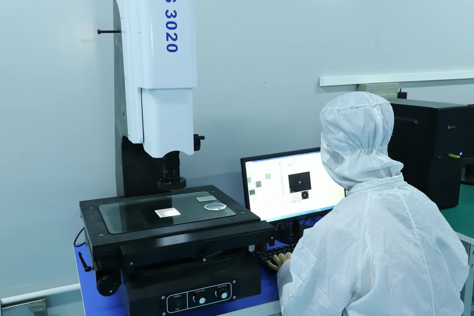
- Miniature Circuit Inspection: Object-Space Pixels and Defect VisibilityTechnology & DesignDesign guide
- Second-Side Ceramic Assembly: Retaining Inverted Components During ReflowTechnology & DesignDesign guide
- Via Metallization Process Interactions: Cleaning, Drying and FiringTechnology & DesignDesign guide
- Edge Termination Deposition: Finding Fixture-Shadow GapsTechnology & DesignDesign guide
- Repeated Soldering on Thick Film Pads: Leaching and Rework LimitsTechnology & DesignDesign guide
- Die-Attach Resin Bleed: Protecting Adjacent Wire-Bond RegionsTechnology & DesignDesign guide
- Ceramic Thermal Paths After Assembly: Where Interface Losses AppearTechnology & DesignDesign guide
- Printing Direction and Narrow-Line Continuity on Ceramic CircuitsTechnology & DesignDesign guide
- Via-Fill Drying Recession and Refill Sequence on Ceramic CircuitsTechnology & DesignDesign guide
- Ceramic Circuit Enclosures: Trapped-Gas Pressure After Lid ClosureTechnology & DesignDesign guide
- Miniature Ceramic Panels: Fixture Release and Transfer DamageTechnology & DesignDesign guide
- Ceramic Via Arrays: Redundancy, Land Area and Test AccessTechnology & DesignDesign guide
- Solid Ground Plane or Separated Returns? Follow the Actual CurrentTechnology & DesignDesign guide
- Strip First or Unit First? Choose the Safer Ceramic Storage StateTechnology & DesignDesign guide
- Wide Bus or Parallel Narrow Conductors on Ceramic CircuitsTechnology & DesignDesign guide
- Route Detour or Dielectric Crossover on a Thick-Film Ceramic CircuitTechnology & DesignDesign guide
- Assembly integration versus replaceable subassembliesTechnology & DesignDesign guide