
On this page
- What does the drawing need to define?
- Confirm the process route for the ordered part
- Define the conductor pattern and finish coverage
- Control coverage at cutouts and openings
- Match each inspection to its feature and layer
- Review the artwork and inspection plan together
- Questions for the design review
- Prepare an engineering RFQ
- Related engineering resources
Prepared by Chipsimple Engineering Team, Engineering and technical content review
Published online November 19, 2026 · Reviewed November 19, 2026
What does the drawing need to define?
A patterned ceramic circuit drawing defines where the conductor belongs and which regions remain exposed ceramic. In Kyocera’s thin-film example, etching forms the conductor pattern and plating follows. If only selected features need a finish, identify those features on the drawing and confirm the method used to restrict finish coverage in the project process documentation.
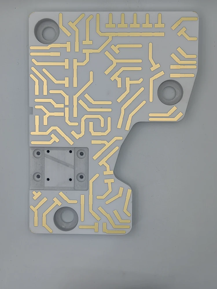
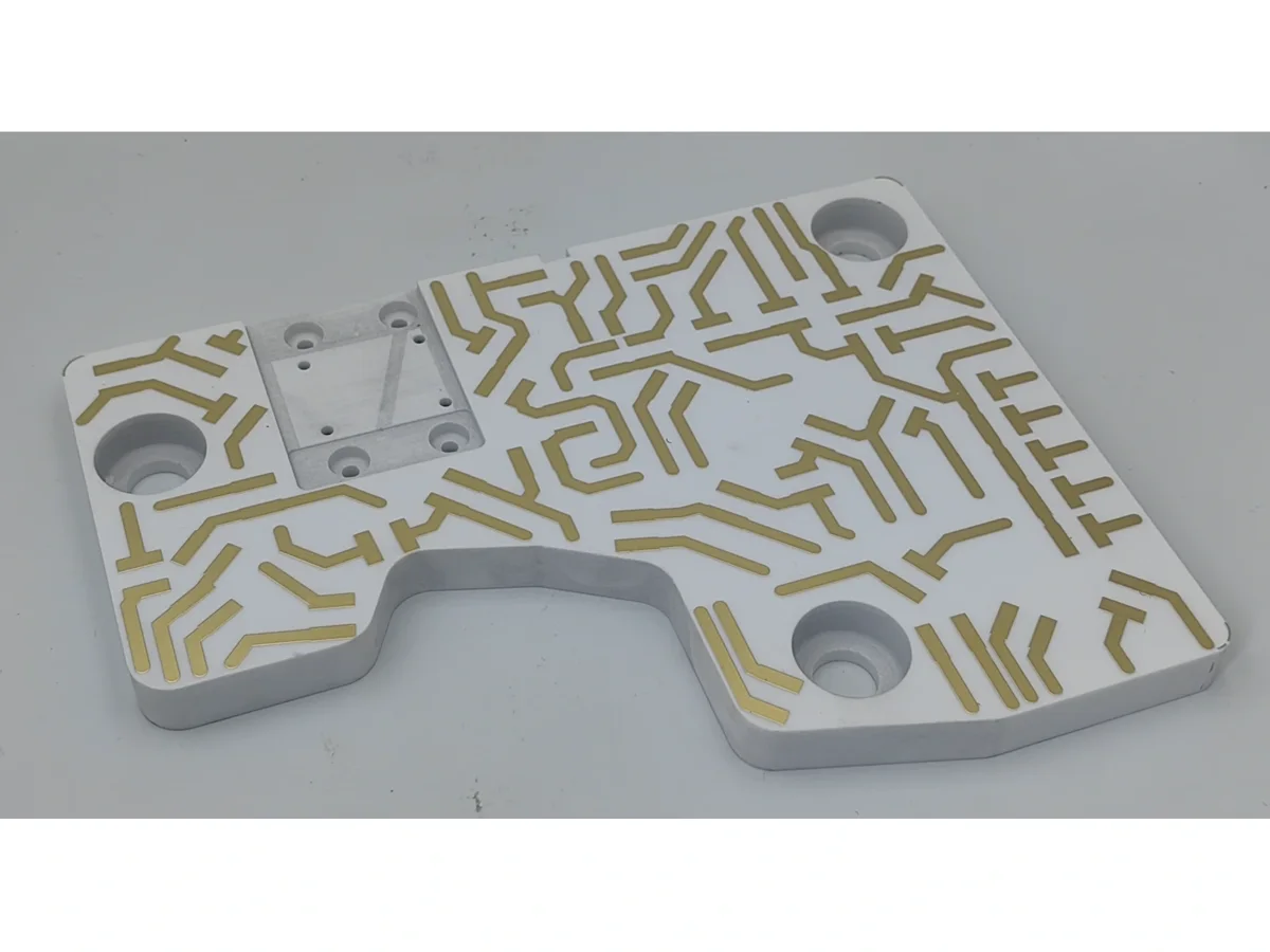
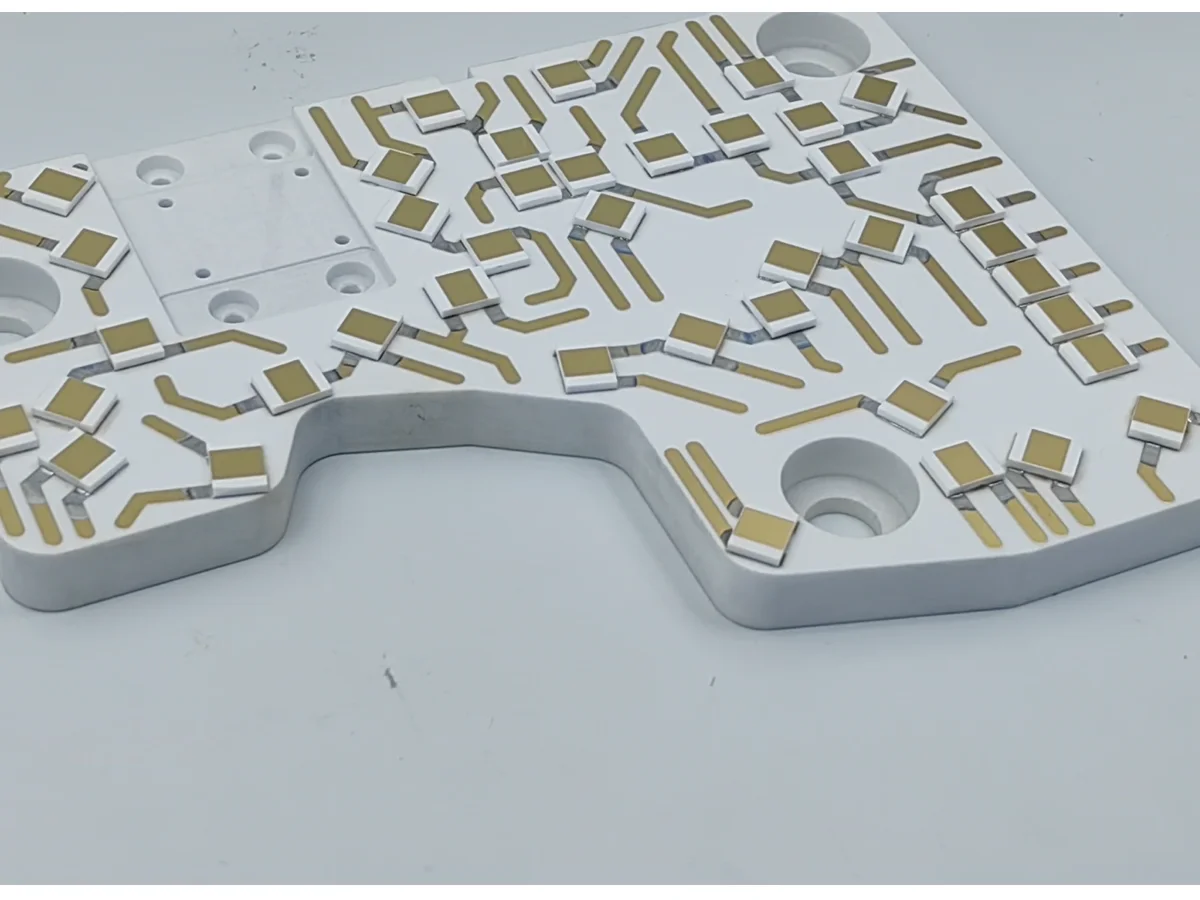
The public BH209A0-1 drawing identifies nickel–gold on selected lead-out areas, pads and optical-path markings on a shaped alumina substrate. Use the cutout and mounting openings in the face-on view to orient the drawing. One oblique view shows the complete substrate outline. An oblique detail view shows the local relationship between visible metallization and the ceramic edge.
Confirm the process route for the ordered part
Kyocera’s example starts with fired ceramic. The surface is ground before a metal film is deposited by evaporation or sputtering. Both single-layer and multilayer ceramic substrates can carry thin film. The project process documentation identifies the route and layer system for the ordered part.
Before comparing process proposals, identify each controlled surface, its viewing direction and the pads, markings or lead-outs on it. The BH209A0-1 nickel–gold callout specifies the finish on identified features. Use the project documents to confirm the underlying layer system, the deposition route and any masking required to achieve the specified coverage.
Define the conductor pattern and finish coverage
In the Kyocera example, photoresist is applied and exposed to define the conductor pattern. Etching removes the unprotected metal, and the resist is then removed. Plating follows, with the plating combination chosen for the required function. Singulation and final inspection follow in this example. This published route describes how the conductor is patterned and that plating follows. It does not identify a technique for confining the finish to a particular subset of features. Ask the supplier to document the proposed coverage controls, including any masking the chosen route requires, against the feature-level finish map.
On the drawing, define the metal pattern by face, local width and position. Then identify where the specified finish must be present. State where the finish and conductor boundaries must coincide. Use a recognizable common feature to register face views and keep terminal numbering consistent when the part is flipped. Identify the reference for each position requirement, whether it is another metal feature, a finished ceramic edge or the underlying conductor.
| Requirement | Record to request | Decision it supports |
|---|---|---|
| Metal pattern near a ceramic edge | Face drawing showing the conductor, finished edge and applicable tolerances | Which physical edge controls the feature position |
| Nickel–gold on selected features | Finish map identifying required regions, bare areas and any section-defined extent. Specify a coverage method that distinguishes the finish from adjoining surfaces at the named inspection locations. | Accept each boundary against the drawing limits and required bare areas. If contrast is inadequate, agree a suitable alternative coverage check. |
| Thickness at a particular pad | Finished feature envelope, intended spot location, positioning allowance, beam footprint, layer model, reference standard and acceptance range | Whether the proposed measurement can verify the specified layer at that location |
Control coverage at cutouts and openings
A pattern-to-pattern tolerance controls the relative location of metal features. A pattern-to-edge tolerance also accounts for the position of the cut ceramic edge. Identify the controlling face and edge on the drawing so the inspection uses the same reference as the requirement.
Use the face-on photo to locate the opening under discussion. Use the controlled face drawing and any applicable section to determine whether the metal must stop short of the edge, terminate at the edge or continue onto another surface. If an opening wall requires coverage, add a detail or section that names the wall, shows the section direction and defines how far the metal extends. Identify any edges that must remain bare.
Match each inspection to its feature and layer
Identify how each finish boundary will be distinguished from the adjacent surface, including the underlying conductor. Use a registered optical comparison with the face drawing only where the agreed method resolves the required finish boundary. Check the boundary against the drawing tolerance and confirm that required bare areas remain bare. If the surfaces cannot be distinguished optically, agree a coverage check capable of resolving the named finish on those features. For a wall extent shown in section, for example, a qualified cross-section check can compare the finish extent at its documented location with the specified limits. Define where to inspect and how the result will be accepted.
Record local thickness checks separately. For a coating thickness requirement, identify the individual feature and the layer to be reported. If X-ray fluorescence (XRF) is proposed, check that the actual beam footprint fits inside the smallest permitted finished region, with allowance for feature size, registration and measurement positioning. For an asymmetric footprint or an angled boundary, check clearance at each limiting edge. A local XRF result records thickness only at its documented spot. A footprint crossing onto adjacent material cannot verify the thickness of the pad alone.
Even when the beam fits within the pad, a thin coating can allow the underlying material to contribute to the spectrum. Record the layer model, reference standard, spot location, acquisition conditions and acceptance range. Counting statistics, measurement time and differences in layer density from the reference can affect the result. Repeat readings characterize repeatability at the selected spot. If a required region cannot accommodate a suitable spot, identify the region and agree on a smaller spot or another suitable method, such as an agreed cross-section.
Review the artwork and inspection plan together
For each controlled region, record the face, feature identifier, conductor boundary, required finish and reference used to check its position. A lead-out and an optical-path marking may have different geometries and inspection requirements. Identify the evidence required for each feature and record the locations covered by any agreed sampling plan.
Request the proposed manufacturing sequence and a feature-level inspection plan. Check that the artwork defines the intended pattern, the process specification identifies the layer system and selective finishing method, and the inspection plan names the measurements and acceptance criteria. For unresolved items, identify the affected feature and the drawing or verification decision needed.
Questions for the design review
Can a nickel–gold callout tell me how the first metal film was deposited?
The callout specifies the finish on the identified features. Check the agreed manufacturing specification for the deposition process, underlying layer system and processing sequence. Kyocera’s evaporation or sputtering example illustrates one possible route.
Should I measure pad position from the neighbouring pad or the ceramic edge?
Use the reference specified for the requirement. Pad-to-pad spacing and clearance to a finished ceramic edge each need their own dimension and tolerance if both affect the assembly.
Will an XRF reading on a wide lead-out cover the narrow marking beside it?
The wide lead-out provides local evidence under the applicable layer model, which must account for contributions from the underlying layers and substrate when relevant. For a narrow marking with its own requirement, assess the actual footprint or agree on another suitable method. Any plan treating the lead-out as representative of the marking needs a documented technical basis and explicit agreement.
Prepare an engineering RFQ
- Face-labelled pattern artwork with viewing directions, common reference features and terminal identifiers
- Controlled substrate outline and thickness, with opening and cutout positions
- Feature-by-feature finish map and required layer stack
- Metal-to-metal and metal-to-finished-edge dimensions and tolerances
- Coverage details for face edges and opening walls, including areas that must remain bare
- Thickness requirements by layer and feature, eligible measurement sites and acceptance criteria
Related engineering resources
Measurement definitions and references
- Kyocera — Manufacturing Process for Thin-Film Ceramic Substrates
- Tecdia Thin Film Ceramic Substrate Design Guide — circuit order data
- Tecdia Thin Film Ceramic Substrate Design Guide — conductor setbacks
- Hitachi High-Tech — XRF for electronics plating
- Hitachi High-Tech — interpreting multilayer XRF coating measurements
- BH209A0-1 Metallized Alumina Substrate — public drawing reference