
On this page
- What the HBM Rows Tell You About 0603
- Set the Scope at the Component and Package Size
- Record Discharge Counts and Acceptance Criteria
- Index the Photographed Patterns Before Requesting Drawings
- Verify the Resistive Branch and Both Discharge Terminals
- Close the Chip Comparison and Substrate Review
- Questions for the design review
- Prepare an engineering RFQ
- Related engineering resources
Prepared by Chipsimple Engineering Team, Engineering and technical content review
Published online November 19, 2026 · Reviewed November 19, 2026
What the HBM Rows Tell You About 0603
For a proposed 0603 chip, the Vishay TNPW e3 thin-film row specifies a 1000 V component human body model (HBM) test level. The Vishay D/CRCW-P e3 thick-film row says the voltage depends on size and gives no numerical level, so whether the test voltages match remains unresolved. Compare the documented HBM procedure, discharge counts by polarity and post-stress resistance-change limits for the two parts.
Keep the post-stress criteria beside the voltage entries. TNPW e3 permits a resistance change of ±(0.5% R + 0.05 Ω), while D/CRCW-P e3 permits ±(1% R + 0.05 Ω). These expressions describe the outcomes each row accepts after its specified stress. A design review should retain both expressions alongside their respective test conditions so that agreement on the procedure and counts cannot be mistaken for agreement on the full test.
Set the Scope at the Component and Package Size
Record the exact proposed part designations and the 0603 package size. The TNPW e3 table assigns levels by package size, so use its 0603 entry for this comparison.
Use these rows for a component HBM comparison. Working voltage and system-level ESD immunity require separate evidence. The D/CRCW-P e3 sheet also lists distinct overload and endurance tests, so use the HBM row when recording discharge conditions and its associated resistance-change criterion. Thin-film and thick-film networks use distinct material and patterning routes. For the broader choice between network routes, see “Thin Film vs Thick Film Resistor Network Selection”. For a custom circuit, confirm the project dimensions, resistor material, fabrication route and applicable ratings against its own records.
Record Discharge Counts and Acceptance Criteria
Record IEC 61340-3-1 HBM for both products. Record the three positive and three negative discharges specified for each product in separate polarity fields. Leave the application order unspecified because the reviewed excerpts give no sequence. Record the tested contact pair only when supporting documentation identifies it.
Copy each resistance-change expression in full, including the fixed 0.05 Ω term. R is the reference resistance used to calculate the percentage term. The reviewed evidence leaves the basis for R unspecified in both rows. Record it as unresolved and confirm the applicable basis before calculating a permitted change. If the same R is used in both expressions, the D/CRCW-P e3 percentage contribution is twice the TNPW e3 contribution. Both expressions include the same fixed 0.05 Ω term. For a design decision, compare the complete permitted change against the circuit’s allowable change and keep the voltage evidence attached to the corresponding part.
| Review field | TNPW e3 thin film | D/CRCW-P e3 thick film |
|---|---|---|
| Component test model | IEC 61340-3-1 HBM | IEC 61340-3-1 HBM |
| Discharges by polarity | Three positive and three negative | Three positive and three negative |
| 0603 test voltage | 1000 V | Numerical level omitted. Obtain the applicable 0603 value. |
| Permitted post-stress resistance change | ±(0.5% R + 0.05 Ω) | ±(1% R + 0.05 Ω) |
| Discharge sequence and contact pair | Unspecified in the reviewed excerpt | Unspecified in the reviewed excerpt |
Index the Photographed Patterns Before Requesting Drawings
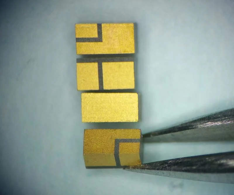
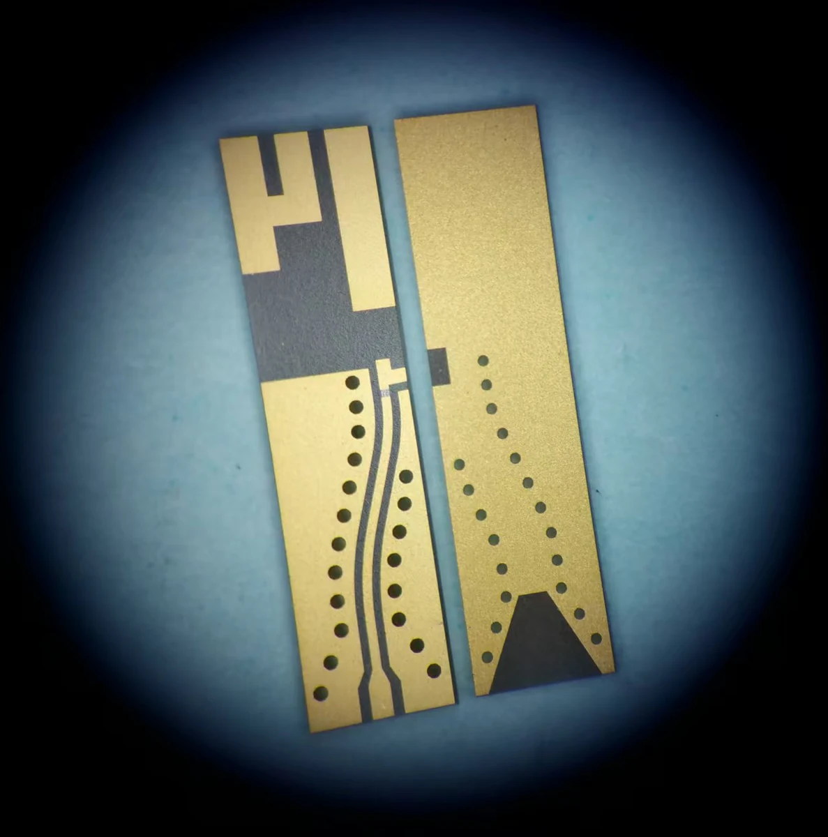
In the four-rectangle view, use the tweezers holding the lowest rectangle to confirm orientation, then index the samples by position from top to bottom. Identify the third rectangle by its position and outline. Where a distinct dark boundary is visible, use it as a secondary locator. Carry those references into the drawing request so each document can be matched to the intended sample. Keep the two strip samples in their own index, using their dark circular features and pattern boundaries to distinguish them.
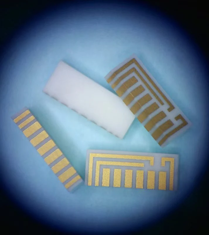
These are examples from our thin-film circuit family. The blue-field view shows folded patterns, repeated strip-shaped areas and outlines on separate samples. These features help request the right drawing for a custom-circuit HBM review. A pattern may contain resistors and conductors or conductors alone. The visible patterned regions alone cannot establish electrical function or a test result for the pictured specimen. Use pad or terminal labels only for features confirmed by the matching artwork. The datasheets provide the 0603 comparison for the two named chip series.
Verify the Resistive Branch and Both Discharge Terminals
Begin with the matching manufactured revision and controlled layer drawings for the indexed sample. If the drawings establish conductor-only artwork at the marked region, record that finding and seek the actual resistor before applying a resistor qualification. If the function is open, request the missing layer and connection evidence. When a resistor is identified, use its artwork and netlist to locate the intended branch. Match it to the actual tested pair named in the specimen-specific HBM test record and its accompanying terminal drawing. A proposed drawing by itself cannot identify the contacts used in a completed test.
Check the construction and revision of the manufactured sample against the HBM test report and its tested terminal pair. A netlist can show a second path across the same terminals. A report covering a discharge across the complete network does not by itself establish the stress on a single branch. For a branch-specific conclusion, obtain evidence in the test record that identifies the tested electrical boundary and addresses any other current paths. Keep the individual branch unqualified while those records are missing.
Close the Chip Comparison and Substrate Review
Ask the thick-film supplier for the applicable 0603 HBM voltage and the document that ties it to the proposed part. If the supplier documents 1000 V, the stated voltage can be recorded as matching the TNPW e3 0603 row. The resistance-change criteria still differ and each must be checked against the design requirement. If the supplier gives a different level, retain the two values explicitly. Until a level is available, keep voltage equivalence open.
For the custom circuit, include the indexed photo reference, the matching artwork and netlist, and the drawing that identifies the tested terminals in the design review. Ask for the applicable HBM evidence tied to that branch and terminal pair, including the documented test level, polarity counts and post-stress criterion. Carry the exact part or drawing identification into the review record so the evidence stays attached to the component or branch to which it applies.
Questions for the design review
Can I use the TNPW e3 0603 voltage for the D/CRCW-P e3 0603?
Use 1000 V for the TNPW e3 0603 entry. Obtain the applicable D/CRCW-P e3 0603 level from its supplier before comparing the voltages.
Does the smaller resistance-change limit establish better ESD performance?
If both expressions use the same reference resistance R, TNPW e3 has the tighter acceptance limit. The reviewed evidence leaves the basis for R unresolved for both rows. Comparing HBM evidence also requires the applied voltage for each part. The acceptance expressions give permitted changes, and test results are needed to determine measured changes.
What makes the photographed pattern relevant to my HBM review?
Its outline helps you request the matching artwork and netlist. For an HBM conclusion, obtain the report for the manufactured configuration and the tested pair of terminals. If the netlist shows another path across the same pair, require test evidence covering the stress boundary of the intended branch before applying a branch-specific result.
Prepare an engineering RFQ
- Exact chip part designation and 0603 package size
- Required component HBM procedure and voltage, with supplier evidence for the proposed size
- Required discharge counts by polarity and applicable post-stress resistance-change limit
- Custom circuit dimensions, specified resistor material and fabrication route
- Sample reference keyed to top-to-bottom position in the four-rectangle view, with visible boundary shapes where present and the tweezers as an orientation cue
- Matching controlled resistor and conductor artwork, netlist and evidence of manufacture for the identified resistor region
- HBM report tied to the manufactured configuration and tested terminal pair, including coverage of any parallel paths when the claim concerns an individual branch
Related engineering resources
- Thin Film vs Thick Film Resistor Network Selection
- Printed Resistor Pulse Loads: Match Pulse Width to the Actual Source Impedance